Nano-Scale Cu Direct Bonding Technology Using Ultra-High Density, Fine Size Cu Nano-Pillar (CNP) for Exascale 2.5D/3D Integrated System
Kang-Wook Lee
†New Industry Creation hatchery Center (NICHe), Tohoku University, 6-6-10 Aza-Aoba, Aramaki, Aoba-ku, Sendai, Miyagi 980-8579, Japan
(Received December 5, 2016: Corrected December 9, 2016: Accepted December 12, 2016)
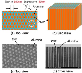
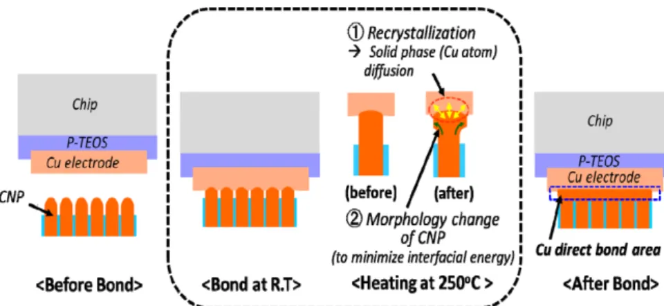
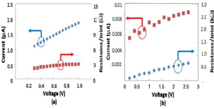
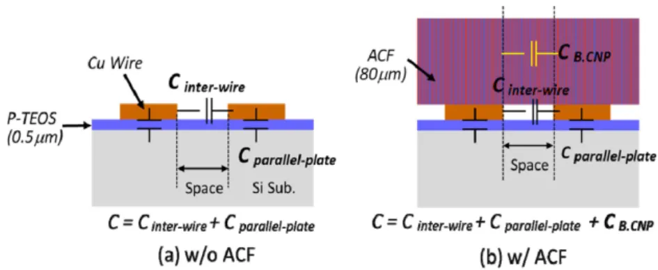
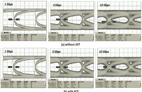
Abstract: We propose nano-scale Cu direct bonding technology using ultra-high density Cu nano-pillar (CNP) with for high stacking yield exascale 2.5D/3D integration. We clarified the joining mechanism of nano-scale Cu direct bonding using CNP. Nano-scale Cu pillar easily bond with Cu electrode by re-crystallization of CNP due to the solid phase diffusion and by morphology change of CNP to minimize interfacial energy at relatively lower temperature and pressure compared to conventional micro-scale Cu direct bonding. We confirmed for the first time that 4.3 million electrodes per die are successfully connected in series with the joining yield of 100%. The joining resistance of CNP bundle with 80µm height is around 30 m for each pair of 10µm dia. electrode. Capacitance value of CNP bundle with 3µm length and 80µm height is around 0.6fF. Eye-diagram pattern shows no degradation even at 10Gbps data rate after the lamination of anisotropic conductive film.
Keywords: nano-scale Cu direct bonding, Cu nano-pillar, esascale 2.5D/3D integration
1. Introduction
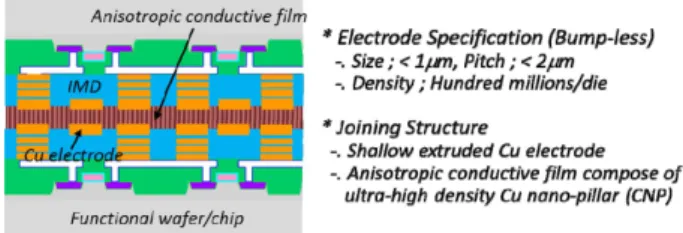
In current high performance 2.5D field-programmable gate array (FPGA) product, a FPGA die has typically 50,000 electro-plated Cu/Sn bumps with 20 µm diameter and 45 µm pitch for joining to a Si interposer.
1)However, ultra-scale 2.5D/3D FPGA requires ultra-high joining den- sity of more than few millions per FPGA die in coming year.
2)Moreover, ultra-high bandwidth memory (3D DRAM) and ultra-high density storage memory (3D Flash) also require ultra-fine joining pitch below 1 µm due to the limited region for TSV array in a die in a future. To meet such requirement, the bump size should be shrunk to 1 µm or sub-µm in diameter. Current standard electro-plated Cu/
Sn pump has been scaled vertically and horizontally by increasing Cu volume and decreasing solder volume. How- ever, it is difficult to scale the bump pitch below 5 µm in current electro-plated Cu/Sn bumping process,
3)especially because of the shrinkage limitation of Sn volume. Some volume of Sn layer is required for solidable joining.
However, Sn layer easily bridge with near bumps if the misalignment accuracy of the chip bonder is larger than 1
µm and if the bonding pressure is too high. Oxide direct and Cu/oxide hybrid bonding technologies have attracted attention as bump-less joining solution to overcome the scaling limitation of electro-plated Cu/Sn bump.
4-7)Cu/
oxide hybrid bonding technology is a more promising solu- tion for ultra-high density 2.5D/3D integration applica- tions, because oxide direct bonding has severe challenges such as the difficulty to etch very thick multilayer of dielectrics for through oxide via (TOV) and huge area penalty due to high density TOVs. However current stan- dard chip-to-wafer (C2W) and wafer-to-wafer (W2W) hybrid bonding technologies have also many challenges such as difficulties to control the good post-CMP (chemi- cal mechanical polishing) topography with no Cu dishing, height uniformity (global/local), surface roughness, CMP reproducibility in all Cu electrodes and the severe control of killer particle, surface oxide layer for gap-free intact bonding to achieve high stacking yield. In this paper, to overcome those issues and to achieve high stacking yield, we propose a novel hybrid bonding technology based on nano-scale Cu direct bonding using ultra-high density Cu nano-pillar (CNP) for exascale 2.5D/3D integration.
†