- 1226 -
P형 실리콘 나노선과 Au 나노입자를 이용한 나노플로팅게이트 메모리소자의 전기적 특성 분석
윤창준*, 염동혁* 강정민* 정동영* 김상식* 고려대학교 전기공학과*
Memory characteristics of p-type Si nanowire - Au nanoparticles nano floating gate memory device
Changjoon Yoon*, Donghyuk Yeom*, Jeongmin Kang*, Dong-Young Jeong*, and Sangsig Kim* Department of Electrical Engineering and Institute of Nano Science, Korea University*
Abstract - In this study, a single p-type Si nanowire - Au nanoparticles nano floating gate memory (NFGM) device is successfully fabricated and characterized their memory effects by comparison of electrical characteristics of p-type Si nanowire-based field effect transistor (FET) devices with Au nanoparticles embedded in the Al2O3 gate materials and without the Au nanoparticles. Drain current versus gate voltage (IDS-VGS) characteristics of a single p-type Si nanowire - Au nanoparticle NFGM device show counterclockwise hysteresis loops with the threshold voltage shift of
∆Vth = 3.0 V. However, p-type Si nanowire based top-gate device without Au nanoparticles does not exhibit a threshold voltage shift.
This behavior is ascribed to the presence of the Au nanoparticles, and is indicative of the trapping and emission of electrons in the Au nanoparticles.
1. 서 론
The nanomaterials such as nanoparticles and nanowires have received attention in recent years. Semiconductor and metal nanoparticles were used as charge storage nodes for memory devices due to their charge confinement effect, which motivates the so-called nano-floating gate memory (NFGM) devices [1]. NFGM structures containing nanoparticles embedded in dielectric layers have attracted a great deal of attention, because of their low voltage operation, good endurance, and fast write/erase speed, compatible process to conventional silicon process technology as well as even better scalability than conventional floating gate memories [2]. Among the metal nanoparticles, Au nanoparticles with a work function of 4.83 eV are expected to be excellent for the charge storage nodes in floating gate memory devices. On the other hand, nanowires have clear advantages when used as a channel of nanodevices as a result of their high crystalline quality, excellent electrical properties and charge transportation characteristics [3]. It is desirable to use hybrid nanostructures consisting of metal nanoparticles incorporated into nanowires to maximize both their charge storage and transportation capabilities. This motivates our research on top-gate single p-type Si nanowire-based NFGM device with floating gate nodes consisting of Au nanoparticles on top of the nanowire channels.
2. 본 론
The full fabrication procedure of p-type Si nanowire - Au nanoparticle NFGM devices developed in this work described below.
At first, for the formation of Au nanoparticles on the p-type Si nanowires, the prepared p-type Si nanowire were coated with an Al2O3 tunneling oxide layer with a thickness of 5 nm using an atomic layer deposition (ALD) method and dispersed in a solution of HAuCl4 (10mL, 0.1M) with the aid of ultrasonication to give a suspension. The suspension was supersonicated for 30 min, aged for 1 hour, and was air-dried at room temperature. Finally, the p-type Si nanowires wrapped highly dispersed Au nanoparticles are obtained by heating them upto 300 ˚C at a rate of 5 ˚C /min and keeping them at that temperature for 1 hour under Ar atmosphere [4].
The p-type Si nanowires wrapped with Au nanoparticles are dispersed on a heavily doped p-type Si substrate capped with a SiO2
layer having a thickness of 300 nm. Then, source and drain electrodes are patterned on a single Si nanowire selected from the dispersed Si nanowires by a photolithographic process under an
optical microscope and etched out Al2O3 layers using H3PO4 solution on the patterned source and drain regions for the contact with the electrode metals. The metal electrodes were formed by the thermal evaporation of Ti (70 nm)/Au (30 nm) and the channel length between the electrodes was 6 μm. The 25nm thickness of Al2O3 layer for control oxide layer was uniformly deposited on the single Si nanowire by the ALD method and Ti (70 nm)/Au (30 nm) are deposited on the channel part of the p-type Si nanowire - Au nanoparticle NFGM device after the patterning of the gate region between the source and drain electrodes by the photolithographic process. For a comparison, a reference device was also prepared by the same processes described above except the process of Au nanoparticles formation. For the more correct comparison, source and drain electrodes are patterned on a single p-type Si nanowire selected from the dispersed p-type Si nanowires by the same fabrication method and Al2O3 layers having a thickness of 5nm and 20 nm are deposited over two steps on the selected Si nanowire by ALD for the formation of a gate dielectric layer. Also, Ti (70 nm)/Au (30 nm) are deposited on the gate region of a single Si nanowire field effect transistor(FET) device.
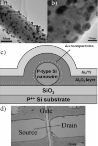
<Fig.1> (a) TEM image and (b) HRTEM image of a selected p-type Si nanowire - Au nanoparticle nanomaterial and (c) the cross-sectional schematic and the (d) microscopy image of the p-type Si nanowire - Au nanoparticle NFGM device.
Figure 1(a) and 1(b) shows transmission electron microscopy (TEM) and high resolution transmission electron microscopy (HRTEM) image of structure of the p-type Si nanowires wrapped Au nanoparticles.
The average particle size of the wrapped Au nanoparticles in the composite p-type Si nanowires is 6 ± 0.5 nm. Also, it noted that the Au nanoparticles are well dispersed on the surface of the p-type Si nanowires without any aggregation. The surface density of the nanoparticles was estimated to be 1.2 × 1012 cm-2. The cross-sectional schematic and the microscopy image of the p-type Si nanowire - Au nanoparticle NFGM device are shown in Fig. 1(c) and 1(d). The cross-sectional schematic exhibits an ideal case of the cross-sectional view of the p-type Si nanowire - Au nanoparticle NFGM device and the microscopy image reveals that top-gate 2008년도 대한전기학회 하계학술대회 논문집 2008. 7. 16 - 18
- 1227 -
<Fig.2> IDS – VDS sweep curves at the various VGS values obtained from (a) the p-type Si nanowire - Au nanoparticle NFGM device and (b) conventional p-type Si nanowire based top-gate FET device without Au nanoparticles
electrode is formed successfully between source and drain electrodes.
The memory mechanism expected for our NFGM devices under this study is briefly described here. The F-N (Fowler-Nordheim) tunneling of holes from the nanowire channel to the nanoparticles happens easily when the gate voltage is negatively biased. These holes are stored within the Au nanoparticles. The valence band offset built at the interface between the Au nanoparticles and the Al2O3
layer at the gate blocks the leakage of the stored holes from the Au nanoparticles to the nanowire channel. On the other hand, the removal of the stored holes occurs when the gate voltage is positively biased. The charging and discharging of the holes is the source of the memory characteristics of the NFGM devices.
The holes are trapped within the deep potential well for the long time due to the valence band offset built at the interface between the Au nanoparticles and the Al2O3 layers. These expected characteristics were confirmed throughout the electrical measurements as shown below.
The various electrical characteristics of p-type Si nanowire - Au nanoparticle NFGM device were measured by an HP4155c semiconductor parameter analyzer (Agilent) and shown in Fig. 2 and 3. The memory effect is characterized by measuring the threshold voltage shift after charging and discharging the Au nanoparticles.
The measured drain current versus drain voltage IDS-VDS curves for the p-type Si nanowire - Au nanoparticle NFGM and reference devices are shown in figures 2(a) and 2(b). The graphs show that the drain current increases linearly with increasing drain voltage. The straight form of the IDS-VDS curves indicates their ohmic characteristics and, the IDS-VDS curves of them are fully depleted by specific positive gate voltages. From these results, we confirmed that the Si nanowires are p-type materials and the majority carrier of our devices is holes.
Figure 3 shows that the IDS-VGS characteristics of p-type Si nanowire - Au nanoparticle NFGM device and without Au nanoparticles as a reference sample under multiple drain voltages of 1V, 0.75V and 0.5V. Figure 3(a) exhibits that Au nanoparticles have been used as charge storage nodes of NFGM device. The behavior of device is remarkably changed when Au nanoparticles are formed on the p-type Si nanowire. Au nanoparticles were charged during the gate voltage sweeping, and the charges in the Au nanoparticles lead to the threshold voltage shift by screening the applied gate voltage.
A threshold voltage shift of 3V is attained at a sweep gate voltage from -10V to 10V. The counterclockwise hysteresis loops of p-type Si nanowire - Au nanoparticle NFGM devices are attributed to the charging and discharging processes of holes in the NFGM devices.
<Fig.3> IDS – VGS sweep curves at the various VDS values obtained from (a) the p-type Si nanowire - Au nanoparticle NFGM device and (b) conventional p-type Si nanowire based top-gate device without Au nanoparticles.
When a negative gate voltage applied to the gate, the charge trapping in the floating gate composed of the Au nanoparticles originates from the injection of holes from the p-type Si nanowire into the Au nanoparticles. When a positive gate voltage applied to the gate, the holes which remained in nanoparticles are extracted.
On the other hand, IDS-VGS curves of conventional p-type Si nanowire based top-gate device without Au nanoparticles which is fabricated as a reference sample are shown a negligible threshold voltage shift which indicates that the effect of the charge traps in the Al2O3 layer or mobile ions is negligible.
3. 결 론
Au nanoparticles can be successfully formed on the surface of the p-type Si nanowires which have coated with 5 nm Al2O3 layer as tunneling oxide and the p-type Si nanowire - Au nanoparticle NFGM device is successfully fabricated by a conventional photolithographic process. From the IDS-VGS curve, counterclockwise hysteresis loops which caused by tunneling of holes from the channel to nanoparticles and 3V threshold voltage shift which is generally obtained from NFGM device are characterized. On the other hand, from the IDS-VGS
curve of p-type Si nanowire based top-gate device without Au nanoparticles, the threshold voltage shift is not obtained, resulting from the absence of charge storage nodes. These results reveal that our p-type Si nanowire - Au nanoparticle NFGM device has a sufficient substitutability for the conventional memory devices.
[참 고 문 헌]
[1] Han, K. Kim, I. Shin, H. J. "Hole and Valence Band Electron Tunneling in a P-Channel Si Nano-Crystal Memory", Korean Phys.
Soc. 37, 907, 2004.
[2] Guo, L. Leobandung, E. Chou, S. Y, "A Silicon Single-Electron Transistor Memory Operating at Room Temperature", Science, 275, 649, 1997.
[3] Cui, Y, Lieber, C. M, "Functional Nanoscale Electronic Devices Assembled Using Silicon Nanowire Building Blocks", Science, 291, 851, 2001.
[4] X. Yan, T. Xu, S. Xu, G. Chen, Q. Xue, S. Yang,
"Polymer-assisted synthesis of aligned amorphous silicon nanowires and their core/shell structures with Au nanoparticles", Chem. Phys.
Lett., 397, 128, 2004