Vol. 26, No. 10 (2016)
556
Comparison of Electrical Properties between Sputter Deposited Au and Cu Schottky Contacts to n-type Ge
Hogyoung Kim 1† , Min Kyung Kim 2 and Yeon Jin Kim 2
1Department of Visual Optics, Seoul National University of Science and Technology, Seoul 01811, Republic of Korea
2Department of Electronic and IT Media Engineering, Seoul National University of Science and Technology, Seoul 01811, Republic of Korea
(Received August 19, 2016 : Revised September 1, 2016 : Accepted September 5, 2016)
Abstract
Using current-voltage (I-V) and capacitance-voltage (C-V) measurements, the electrical properties of Au and Cu Schottky contacts to n-Ge were comparatively investigated. Lower values of barrier height, ideality factor and series resistance were obtained for the Au contact as compared to the Cu contact. The values of capacitance showed strong dependence on the bias voltage and the frequency. The presence of an inversion layer at the interface might reduce the intercept voltage at the voltage axis, lowering the barrier height for C-V measurements, especially at lower frequencies. In addition, a higher interface state density was observed for the Au contact. The generation of sputter deposition-induced defects might occur more severely for the Au contact; these defects affected both the I-V and C-V characteristics.Key words
barrier height, series resistance, interface state.1. Introduction
Germanium has gained significant interest as one of the potential materials to replace Si in complementary metal-oxide-semiconductor(CMOS) devices, due to its higher electron and hole bulk mobilities than Si.
1)With scaling down CMOS devices continually, it is essential to minimize the parasitic resistance in metal source/drain(S/
D) junction. Despite the progress, rapid advances in Ge based device performances has been limited due to strong Fermi level pinning(FLP) at the charge neutrality level(CNL) located close to the valence band edge in Ge.
2,3)This FLP, arising from interface states, produces high Schottky barrier height(SBH) and makes it difficult to reduce the parasitic resistance.
4)Previous research has demonstrated the Fermi level depinning by introducing a thin insulating layer such as Al
2O
3, GeO
x, and TiO
2.
5-7)Metallization is one of important process steps in device fabrication. Electron beam evaporation and sputtering which is possible to deposit high melting point metals, are normally used. However, these methods inevitably introduce some defects in semiconductor. The introduction of defects in Ge layer during metal deposition has been
reported.
8-10)The defects are generated when energetic particles impinge on the semiconductor surface and can alter the barrier height of the contacts.
11)These works were focused on revealing the origin of defect using deep level transient spectroscopy(DLTS). Meanwhile, compari- son of electrical properties of Schottky diodes with different contact metals is beneficial to understand the underlying formation mechanism in metal-semiconductor (MS) contacts. Previous works, however, mainly took place to clarify the origin of FLP effect,
2,4)and detailed comparison of current-voltage(I-V) and capacitance-voltage (C-V) characteristics with different contact metals are rarely done so far. In this regard, we compared the I-V and C- V characteristics between sputter deposited Au and Cu Schottky contacts to n-type Ge. Here, two Schottky metals were selected because Au(5.1 eV) and Cu(4.65 eV) have relatively high and low work functions, respectively.
12)2. Experimental
Single-side-polished Sb-doped Ge (100) wafer(thickness of 500 μm and carrier concentration of ~1 × 10
16cm
–3) was used in this work. Both Au and Cu Schottky con-
†
Corresponding author
E-Mail : [email protected] (H. Kim, Seoul Nat’l Univ. Sci. Technol.)
© Materials Research Society of Korea, All rights reserved.
This is an Open-Access article distributed under the terms of the Creative Commons Attribution Non-Commercial License (http://creative-
commons.org/licenses/by-nc/3.0) which permits unrestricted non-commercial use, distribution, and reproduction in any medium, provided the
original work is properly cited.
tacts(thickness = 100 nm, diameter = 500 μm) were de- posited by radio-frequency(RF) magnetron sputtering through a shadow mask onto two samples after solvent cleaning. Then, ohmic contact was achieved by depositing Al metal(thickness = 150 nm) over the entire back surface of the samples. Current-voltage(I-V) and capacitance- voltage(C-V) measurements were carried out at room temperature with a Keithley 238 current source and an HP 4284A LCR meter.
3. Results and Discussion
Fig. 1 shows the linear I-V characteristics for both contacts. For Au contact, the reverse bias currents seem to increase more rapidly with the reverse bias, indicating the presence of other transport mechanism than thermionic emission(TE). Based on the TE model,
13)the forward bias I-V characteristics were analyzed. The effective barrier heights were determined to be 0.59(± 0.03) and 0.65 (± 0.03) eV, for Au and Cu contacts, respectively. The ideality factors were found to be 1.54(± 0.23) and 2.63 (± 0.86), for Au and Cu contacts, respectively. Higher ideality factor than unity can be due to the presence of interfacial states and an insulator layer at the MS in- terface, and the tunneling current mechanism.
14)The values of series resistance(R
S) can be determined from the slope of the following equations
15)dV / d(ln I) = nkT / q + IR
S, (1) H(I) = V − (nkT / q) ln(I / AA
**T
2), (2) where H(I) is given by H(I) = nφ
B+ IR
S, A is the diode area, A
**is the effective Richardson constant(140 Acm
−2K
−2for n-type Ge), φ
Bis the effective barrier height, n is the ideality factor, and R
Sis the series resistance. Fig. 2
shows dV/d(lnI) vs. I and H(I) vs. I plots for one diode from Cu contact, and similar analyses were performed on other diodes. The average R
Svalues were found to be about 110 and 250 Ω, respectively, for Au and Cu contacts.
Series resistance can result from the semiconductor layer, and the presence of an interfacial layer and interface states. Because two contacts were prepared with the same configuration except Schottky contact metals, the higher series resistance for Cu contact may be due to the presence of an interfacial layer or interface states.
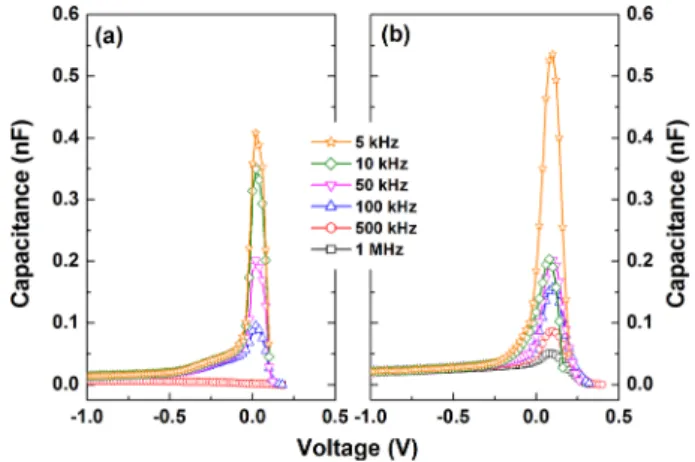
Fig. 3 shows the typical C-V characteristics for both contacts. At low frequencies, the interface states can follow the ac signal and thus, the interface state capaci- tance appeared in parallel with the depletion capacitance, resulting in a higher total capacitance. At sufficiently high frequencies, the interface states can hardly follow the ac signal, making the contribution of interface states to the total capacitance to be negligibly small.
16)The C- V characteristics exhibited an anomalous peak in the forward-bias region, which was attributed to either a distribution of interface states in the band gap, the series
Fig. 1. Linear current-voltage(I-V) characteristics for (a) Au and (b) Cu Schottky contacts to n-Ge. The insets in (a) and (b) present the semilogarithmic current-voltage( I-V) characteristics for Au and Cu contacts, respectively.
Fig. 2. Plots of dV/d(lnI) vs. I and H(I) vs. I for one diode from Cu contact.
Fig. 3. Capacitance-voltage(C-V) characteristics for (a) Au and (b)
Cu Schottky contacts to n-Ge.
resistance, the presence of interface states, and partly due to the injected minority carriers from the non-ohmic back contact.
17,18)Overall, the capacitance values were found to increase with decreasing reverse bias voltage.
Under reverse bias condition, the capacitance of a Schottky junction is described through the following relation
13), (3)
where V
biis the built-in potential, N
Dis the donor con- centration, ε
Sis the relative dielectric constant of the semiconductor, and ε
0is the permittivity of free space.
The barrier height and the carrier concentration can be extracted from a linear plot of A
2/C
2vs. V(see Fig. 4) and the depletion width(W
D) can be obtained from W
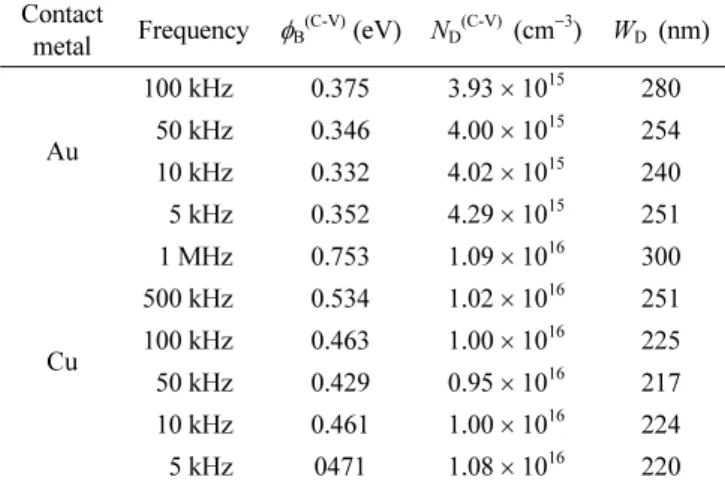
D= . Table 1 shows the calculated electrical parameters from C-V measurements. For both contacts, the carrier concentration is independent of the measure-
ment frequency. The carrier concentration for Cu contact is similar to the value provided by the manufacturer, but that is lower for Au contact. Compared to the homo- geneous barrier height of 0.70 eV for Cu contact that is obtained from the linear fitting to the plot of barrier height vs. ideality factor,
19)the barrier height from C-V measurements at 1 MHz is quite similar. At this fre- quency, the effect of interface states is negligibly small.
For all other conditions, however, the barrier heights from C-V measurements are lower than those obtained from I-V measurements, which are opposite to the normal observation in Schottky diode. Similar lower barrier heights from C-V measurements than those from I-V measurements were observed for Ni/n-Ge Schottky contacts.
20)Although C-V measurements are less prone to the interface states, these defects can alter the depletion width and hence the intercept voltage on the V axis(V
i).
As shown in Table 1, the depletion width decreased at lower frequencies. In Pt germanide/n-Ge Schottky contacts, considerably lower V
ivalues than the calculated values were obtained and this was attributed to a substantial voltage drop across the inversion layer where the electrical field is less sensitive to the external bias.
21)However, further investigation is required to understand the exact origin.
The N
Dvalue in Eq. (3) actually indicates the ionized impurity density in the depletion region. The ionized shallow-level donors in the depletion region are positively charged and some amount of them can be compensated by deep-level acceptor impurities that are negatively charged when occupied by electrons. Using DLTS mea- surements, Auret et al. showed that the electron traps introduced in n-Ge during sputter deposition of Au Schottky contacts are related to interstitial-impurity com- plexes and are located close to the MS interface.
22)They also suggested that the defects observed beyond 100 nm from the surface reached that location by diffusion and
A2⁄C2 2 Vbi–kT q V⁄ –qNDεSε0 ---
⎝ ⎠
⎛ ⎞
=
2εSε0Vbi⁄qND
Fig. 5. Energy distribution of interface state density for both contacts.
Fig. 4. A
2/ C
2vs. V plots for (a) Au and (b) Cu Schottky contacts to n-Ge.
Table 1. Extracted electrical parameters for Au and Cu Schottky contacts to n-Ge from C-V measurements.
Contact
metal Frequency φ
B(C-V)(eV) N
D(C-V)(cm
−3) W
D(nm) Au
100 kHz 0.375 3.93 × 10
15280
50 kHz 0.346 4.00 × 10
15254
10 kHz 0.332 4.02 × 10
15240
5 kHz 0.352 4.29 × 10
15251
Cu
1 MHz 0.753 1.09 × 10
16300
500 kHz 0.534 1.02 × 10
16251
100 kHz 0.463 1.00 × 10
16225
50 kHz 0.429 0.95 × 10
16217
10 kHz 0.461 1.00 × 10
16224
5 kHz 0471 1.08 × 10
16220
their concentration is not a fair reflection of the defects produced by sputter deposition close to the interface. The higher current value of Au Schottky contacts formed by sputter deposition as compared to resistively deposited Au contacts was associated with the process-induced defects.
11)Then, it can be inferred that the deposition- induced defects are generated more severely for Au contact compared to Cu contact.
The distribution of interface state density(D
it) of a Schottky junction can be determined from measured low frequency(C
LF) and high frequency(C
HF) capacitances through the following relation
23), (4)
where Ψ
Sis the surface potential. Here, C
LFand C
HFcapacitances were taken from the values measured at 5 kHz and 1 MHz, respectively. The energy distribution of interface states in Fig. 5 shows higher D
itvalues for Au contact. With decreasing interface state density, the higher barrier height was found in metal/n-GaN Schottky junctions.
24)Hence, the lower barrier height for Au contact can be due to the higher interface state density. These interface states might also increase the reverse leakage current as shown in Fig. 1. Finally, the results from Fig.
5 indicate that the higher ideality factor and the higher series resistance for Cu contact are due to the presence of an interfacial layer rather than the interface states.
Previous research reported that the chemical treatments such as conventional hydrogen fluorine(HF), hydrogen chlorine(HCl) and hydrogen bromine(HBr) cannot remove effectively the native oxide GeO
xon Ge surface.
25,26)Even after such chemical treatments, Ge surface can be easily re-oxidized in air.
27)Hence, it is possible that native GeO
xis present on the Ge surface before metal deposition. Probably, this native oxide was not removed well during Cu deposition, working as an interfacial layer.
On the contrary, the native oxide was removed more effectively during Au deposition. However, the exact origin of the interfacial layer needs further investigation.
4. Conclusion
In conclusion, we performed electrical characterization of Au and Cu Schottky contacts to n-Ge using current- voltage(I-V) and capacitance-voltage(C-V) measurements.
Compared to Cu contact, I-V data for Au contact pro- duced lower barrier height and ideality factor. The values of capacitance showed strong dependence on bias voltage and frequency. The presence of an inversion layer at the interface reduced the intercept voltage on the voltage
axis. Due to this, probably lower barrier heights from C- V measurements(especially at lower frequencies) were obtained as compared to those from I-V measurements.
During the sputter deposition, interface states were generated more severely for Au contact and some of these defects might diffuse into Ge layers.
References
1. H. Shang, M. Frank, E. Gusev, J. Chu, S. Bedell, K.
Guarini and M. Jeong, IBM J. Res. Dev., 50, 377 (2006).
2. A. Dimoulas, P. Tsipas, A. Sotiropoulos and E. Evangelou, Appl. Phys. Lett., 89, 252110 (2006).
3. D. Kuzum, K. Martens, T. Krishnamohan and K.
Saraswat, Appl. Phys. Lett., 95, 252101 (2009).
4. T. Nishimura, K. Kita and A. Toriumi, Appl. Phys. Lett., 91, 123123 (2007).
5. Y. Zhou, M. Ogawa, M. Bao, W. Han, R. Kawakami and K. Wang, Appl. Phys. Lett., 94, 242104 (2009).
6. T. Nishimura, K. Kita and A. Toriumi, Appl. Phys. Exp., 1, 051406 (2008).
7. B. Tsui and M. Kao, Appl. Phys. Lett., 103, 032104 (2013).
8. F. Auret, W. Meyer, S. Coelho and M. Hayes, Appl. Phys.
Lett., 88, 242110 (2006).
9. E. Simoen, K. Opsomer, C. Claeys, K. Maex, C.
Detavernier, R. Meirhaeghe and P. Clauws, J. Electrochem.
Soc., 154, H857 (2007).
10. S. Coelho, F. Auret, P. Rensburg and J. Nel, J. Appl.
Phys., 114, 173708 (2013).
11. F. Auret, S. Coelho, P. Rensburg, C. Nyamhere and W.
Meyer, Mater. Sci. Semicond. Process., 11, 348 (2008).
12. H. Michaelson, J. Appl. Phys., 48, 4729 (1977).
13. S. M. Sze, Physics of Semiconductor Devices, 2nd Ed., Wiley, New York (1981).
14. J. Sullivan, R. Tung, M. Pinto and W. Graham, J. Appl.
Phys., 70, 7403 (1991).
15. S. Cheung and N. Cheung, Appl. Phys. Lett., 49, 85 (1986).
16. S. Witczak, J. Suehle and M. Gaitan, Solid State Electron., 35, 345 (1992).
17. P. Chattopadhyay and B. Raychaudhuri, Solid State Electron., 36, 605 (1993).
18. M. Green and J. Shewchun, Solid State Electron., 16, 1141 (1973).
19. W. Mönch, J. Vac. Sci. Technol. B, 17, 1867 (1999).
20. A. Chawanda, J. Nel, F. Auret, W. Mtangi, C. Nyamhere, M. Diale and L. Leach, J. Korean Phys. Soc., 57, 1970 (2010).
21. H. Yao, D. Chi, R. Li, S. Lee and D. Kwong, Appl.
Phys. Lett., 89, 242117 (2006).
22. F. Auret, S. Coelho, W. Meyer, C. Nyamhere, M. Hayes and J. Nel, J. Electron. Mater., 36, 1604 (2007).
23. S. Chattopadhyay, K. Bera, K. Ray, K. Bose, D. Dentel and L. Kubler, J. Mat. Sci. Mater. Electron., 9, 403 (1998).
Dit qεSNd⁄2ψS CLF–CHF qCHF ---
⎝ ⎠
⎛ ⎞
=
24. M. Mamor, J. Phys. Condens. Matter., 21, 335802 (2009).
25. S. Sun, Y. Sun, Z. Liu, D. Lee, S. Peterson and P.
Pianetta, Appl. Phys. Lett., 88, 021903 (2006).
26. X. Li, A. Li, X. Liu, Y. Gong, X. Chen, H. Li and D.
Wu, Appl. Surf. Sci., 257, 4589 (2011).
27. B. Xue, H. Chang, B. Sun, S. Wang and H. Liu, Chin.
Phys. Lett., 29, 046801 (2012).