Design and Performance Evaluation of On-chip Antenna for Ultra Low Power Wireless Transceiver
5
0
0
전체 글
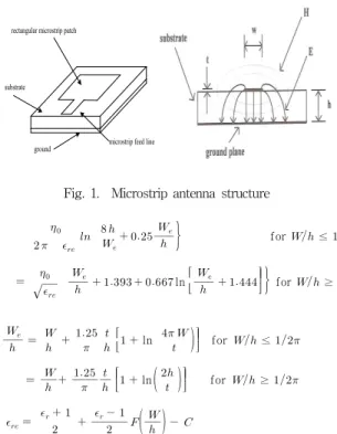
(2)
(3)
(4)
(5)
수치


관련 문서
For the structural design methodology to be practically used for the design of spaceborne electronics, it shall provide more reliable results on the mechanical safety
Performance evaluation of Volume PTV based on Affine Performance evaluation of Volume PTV based on Affine Performance evaluation of Volume PTV based on Affine Performance
Separate instruction/data memory ports 32-bit ARM & 16-bit THUMB instruction set support. Coprocessor interfaces for FP and DSP
Dimensions 85mm x 56mm, Chip Broadcom BCM2835 SoC full HD multimedia applications processor, CPU 700 MHz Low Power ARM1176JZ-F Applications Processor, GPU Dual Core
In compact rectenna design, wireless power transmission technology is expected to be low power and low voltage in order to drive wireless
In this study, using a coplanar waveguide employing Periodic Strip Structure (PSS), highly miniaturized on-chip Wilkinson power divider was realized on silicon
2) Electronics and information technology: smaller ICs on-a-chip, faster computers, increased memory / quantum bits to store more data in smaller computers /
Chip which allows to check gene expression or mutation by adhering highly integrated Oligonucleotide, cDNA, genomic DNA, etc..
