1. Introduction
Recently, thin-film solar cells have been investigated intensively as a possible alternative for bulk Si solar cells. Among thin-film solar cells, polycrystalline silicon (poly-Si) thin-films are attractive as photovoltaic materials because of no light-induced degradation, high carrier mobility, and low-cost production. A number of poly-Si crystallization methods, such as SPC (solid phase crystallization) and epitaxial growth after fabricating poly-Si seed layer using aluminum induced crystallization (AIC), have been investigated, especially in the field of poly-Si thin-film solar cells1-6). In 2007, CSG Solar developed a crystalline silicon on glass (CSG) method based on SPC with a module efficiency of above 10%1,2). Even though the CSG method based on SPC has high efficiency, it has a long processing time and small grain size of about 1 µm. To make large-grained poly-Si films for thin-film solar cells, epitaxial growth on a poly-Si seed layer using AIC has been proposed. Gordon et al. reported 8%
efficient thin-film poly-Si solar cells based on AIC and atmosphere
pressure chemical vapor deposition (APCVD)4,5). However, the APCVD at a high temperature above 1000°C is unsuitable for low-cost glass substrates, and the high density of defects by Al contamination at the seed layer leads to increased recombination.
Therefore, it is necessary to lower the process temperature and Al contamination.
In this work, to overcome the limitations mentioned above we propose epitaxial growth of large-grained poly-Si film on a vapor induced crystallization (VIC) processed poly-Si seed layer using hot-wire CVD. Eom et al. reported high-quality poly-Si films by crystallization of a-Si in NiCl2 and AlCl3 vapor instead of Al metal deposition for thin-film transistors (TFTs)7-9). By the VIC process large poly-Si grains are achieved and the Al contamination is much lower than that by the conventional Al layer conversion method. An epitaxial Si film was grown at low temperature using Al-induced crystal growth (AICG) by Ahn et al.10).
In this paper, we apply a very-thin seed Si layer fabricated by the VIC process with AlCl3 vapor for the epitaxial growth of p-type Si film at low temperature with the help of AICG. We characterize the p-type Si film grown by the AICG method and apply it to thin-S film solar cells.
Epitaxial Growth of Boron-doped Si Film using a Thin Large-grained Si Seed Layer for Thin-film Si Solar Cells
Seung Mo Kang1,2) ․ Kyung Min Ahn1) ․ Sun Hong Moon1) ․ Byung Tae Ahn1)*
1)Department of Materials Science and Engineering, Korea Advanced Institute of Science and Technology, Daejeon 305-701, South Korea
2)Present address: Samsung SDI, Cheonan, Korea
ABSTRACT: We developed a method of growing thin Si film at 600°C by hot wire CVD using a very thin large-grained poly-Si seed layer for thin-film Si solar cells. The seed layer was prepared by crystallizing an amorphous Si film by vapor-induced crystallization using AlCl3
vapor. The average grain size of the p-type epitaxial Si layer was about 20 µm and crystallographic defects in the epitaxial layer were mainly low-angle grain boundaries and coincident-site lattice boundaries, which are special boundaries with less electrical activity.
Moreover, with a decreasing in-situ boron doping time, the mis-orientation angle between grain boundaries and in-grain defects in epitaxial Si decreased. Due to fewer defects, the epitaxial Si film was high quality evidenced from Raman and TEM analysis. The highest mobility of 360 cm2/V·s was achieved by decreasing the in-situ boron doping time. The performance of our preliminary thin-film solar cells with a single-side HIT structure and CoSi2 back contact was poor. However, the result showed that the epitaxial Si film has considerable potential for improved performance with a reduced boron doping concentration.
Key words: Polycrystalline Si film, epitaxial growth, Al-induced crystal growth, vapor induced crystallization
*Corresponding author: [email protected]
Received January 20, 2014; Revised January 28, 2014;
Accepted February 10, 2014
ⓒ 2014 by Korea Photovoltaic Society
This is an Open Access article distributed under the terms of the Creative Commons Attribution Non-Commercial License (http://creativecommons.org/licenses/by-nc/3.0)
which permits unrestricted non-commercial use, distribution, and reproduction in any medium, provided the original work is properly cited.
1
2. Experimentals
2.1 Seed layer preparation
A 100-nm thick a-Si film was deposited by low pressure chemical vapor deposition at 550°C with SiH4 and H2 on a 500-nm thick SiO2 substrate grown on a Si (100) wafer by wet oxidation at 1050°C. The sample was cleaned by ultrasonic cleaning in an acetone and methanol solution for 15 min and then the sample and AlCl3 powder were placed in a two-zone furnace. The 100-nm thick a-Si film was annealed at 530°C for 10 h by supplying AlCl3 vapor at 200°C at a Ar flow of 5 sccm, which is known as vapor-induced crystallization (VIC) process7,8).
2.2 Growth of p-type epitaxial Si film
Metal residue and surface double oxide on the sample after the VIC process were removed in a H2SO4/H2O2 solution and subsequently in a 5% HF solution. Then, the sample was immediately loaded into an HWCVD chamber. A p-type crystal Si film with a thickness of 1.75 μm was grown by HWCVD at 600°C using 20% diluted SiH4 and 1% diluted B2H6 in He as a function of in-situ boron doping time on the poly-Si seed layer.
To make the back surface field layer, boron was doped at the initial stage of the epitaxial growth. The doping concentration of boron was 2500 ppm. In the HWCVD system, W-shaped tantalum wire with a diameter of 0.5 mm was positioned 4.5 cm away from the substrate. The base pressure was under 2x10⁻⁶ Torr and the working pressure was maintained at 50 mTorr during the growth of the epitaxial layer.
2.3 Film characterization
The surface morphology, crystallinity, microstructure, and grain boundary angle were investigated using scanning electron microscopy (SEM), electron backscattered diffraction (EBSD), Raman spectroscopy, and transmission electron microscopy (TEM). A secondary ion mass spectroscopy (SIMS) was performed to investigate the boron doping profile in the poly-Si films. The mobility and resistivity of the poly-Si films were determined by Hall-effect measurements.
2.4 Si film fabrication
We designed a new Si thin-film cell with a hetero-interface front side and CoSi2 back contact. The details of the structure and results are described in the discussion section.
3. Results and discussions
3.1 Characterization of p-type epitaxial Si film Fig. 1 shows the low- and high-magnified SEM images of epitaxial poly-Si thin films grown with various in-situ boron doping conditions: 0 ppm for 60 min (a,b), 0 ppm for 55 min after 2500 ppm for 5 min (c,d), and 2500 ppm for 60min (e,f).
After grain boundary etching with a diluted Secco etchant (CrO3/49% HF/H2O = 0.75:1:100 M), the grain boundaries were clearly visible.
The brightness through grain boundaries can easily differentiate grains and grain boundaries in the SEM images. The dark and bright zones of the SEM images correspond to the grains and grain boundaries, respectively. In general, the microstructures of the n-type epitaxial Si layer shown in Fig. 1 are similar to those of a seed poly-Si layer. However, as the in-situ boron doping time increased, the grain size decreased slightly and the bright regions of SEM images increased. In Figs. 1e and 1f, the area of the bright region increased even on the grains. That means that the films have many etching holes because of more defects with the increasing in-situ boron doping concentration.
On the other hand, most grains of Figs. 1a-1d have poly-Si grains with many fewer defects. It is clear that the quality of the
Fig. 1. The low- and high-magnified SEM images of B-doped epitaxial Si films at the following doping conditions: 0 ppm for 60 min (a,b), 0 ppm for 55 min after 2500 ppm for 5 min (c,d), and 2500 ppm for 60 min (e,f)
Si film is better with less B doping.
The crystallographic properties of the poly-Si film were investigated using EBSD. EBSD measurements revealed the size and orientation of the grains in the poly-Si thin-films. Fig.
2 shows the orientation imaging micrographs (OIMs) of boron- doped epitaxial poly-Si films with the following doping conditions:
(a) 0 ppm for 60 min, (b) 0 ppm for 55 min after 2500 ppm for 5 min, and (c) 2500 ppm for 60 min. The color codes of the OIM images show the crystallographic orientation of the grains in the films. All three samples have similar grain-size distribution and show preferential (001) and (111) orientations.
Only a few (110) planes have were detected, which is contrary to what is commonly reported for fine-grained poly-Si films grown by CVD at high temperature11). In the samples, the grain size of most of the grains is in the range of 15 to 30 μm and the average grain size is about 20 μm. Since the grain size of the epitaxial layer is controlled by that of the seed layer, we believe that the grain size is similar regardless of the in-situ boron doping time because the seed layers used in our experiment have the same grain size.
Fig. 3 shows the distribution of the mis-orientation angle as deduced from the OIM images of boron-doped epitaxial poly-Si films with the following doping conditions: (a) 0 ppm for 60 min, (b) 0 ppm for 55 min after 2500 ppm for 5 min, and (c) 2500 ppm for 60 min. There are two main mis-orientations: low-angle grain boundaries (LAGBs) with less than 2° and coincident-site lattice boundaries (CSLs) with high angle. CSL boundaries are mainly twin boundaries of the first order (Σ3), second order (Σ9),
and third order (Σ27)8). As shown in Fig. 3, regardless of boron doping conditions, many LAGBs and a few twin boundaries, such as Σ3, Σ9, and Σ27, which have the low energy levels with special boundaries, exist in all three samples12,13). The average mis-orientation angle of 5-min boron doping (Fig. 3b) was the smallest among the three samples. Therefore, it seems that the low boron doping in poly-Si film will be good for device characteristics even though it has grain boundaries.
Raman spectroscopy was used to evaluate the crystalline quality of the poly-Si film. Fig. 4 shows the Raman spectra of the epitaxial poly-Si films with various boron doping conditions. As
Fig. 2. OIM images of B-doped epitaxial Si films with the following doping conditions: 0 ppm for 60 min (a), 0 ppm for 55 min after 2500 ppm for 5 min (b), and 2500 ppm for 60 min (c)
Fig. 3. The mis-orientation angles in B-doped Si films with the following doping conditions: 0 ppm for 60 min (a), 0 ppm for 55 min after 2500 ppm for 5 min (b), and 2500 ppm for 60 min (c)
Fig. 4. Raman spectra of the B-doped epitaxial Si films as a function of in-situ boron doping time
a reference, a single crystalline Si (c-Si) wafer was also measured.
C-Si wafer has a sharp peak at a wave number of 520 cm-1 with a full width at half maximum (FWHM) of 5 cm-1. Defects and disorders in Si can lead to broadening of the peak. The wave number of the epitaxial Si films was 521cm-1 for all the samples.
FWHM indicates the crystalline quality for poly-Si films. The FWHM values of the samples grown with doping conditions 0 ppm for 60 min (a), 0 ppm for 55 min after 2500 ppm for 5 min (b), 0 ppm for 50 min after 2500 ppm for 10 min (c), 0 ppm for 45 min after 2500 ppm for 15 min (d), and 2500 ppm for 60 min (e) were 7.16, 6.31, 7.42, 7.52, and 11.53 cm-1, respectively.
With an increasing in-situ boron doping time, the FWHM of the Raman peak increased, and the FWHM of the Raman peak with 5-min boron doping was the smallest among the samples. On the other hand, in heavily boron-doped poly-Si film, the Raman peak was distorted and broadened asymmetrically. It has been reported that a resonant interaction between optical phonons and direct intra-band transitions, known as a Fano resonance, causes the distortion14,15).
Cross-sectional TEM images were taken to investigate the crystal quality of the poly-Si thin-films. Fig. 5 shows dark-field cross-sectional TEM images and a selective area diffraction pattern (SADP) of in-situ boron doped epitaxial poly-Si thin-films with the following doping conditions: (a) 0 ppm for 60 min, (b) 0 ppm for 55 min after 2500 ppm for 5 min, and (c) 2500 ppm for 60 min. The lateral grain size of all the poly-Si films with an epitaxial layer grown on the VIC processed poly-Si seed layer was over 3 μm, and the SADPs of all the samples show only spot
patterns. For low boron doping (Fig. 3b), the SADP was well arranged with large spots, indicating that the film is a quasi- monocrystalline state with a low-angle grain boundary. For heavy boron doping, the SADP shows higher-order satellite spots between large spots, indicating that a periodic array of stacking faults exists in the epitaxial poly-Si film. It has been reported that the stacking fault causes the breakdown of epitaxial growth and roughening of the surface16). In addition, a large density of intra-grain defect was found in the heavily boron doped poly-Si thin-film. Therefore, the crystallinity of the heavily boron doped poly-Si film is poor, which is in agreement with the result of the Raman analysis in Fig. 4.
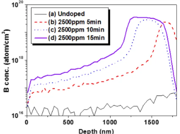
To investigate the boron concentration in poly-Si film, SIMS analysis was performed. Fig. 6 shows the SIMS depth profiles of boron in the epitaxial Si film with various doping conditions.
The boron concentration at the epitaxial Si/ seed layer interface was about 3x1019 cm-3 during in-situ boron doping. The boron concentration in the film decreased as depth decreased. The doing concentration near the film surface was in the range of 7x1016 cm-3 and 3x1018 cm-3, which is too high to be used as an active p-type base layer. The p+ to p transition at the depths of 1.2, 1.3, and 1.5 μm was sharp with doping times of 15, 10, and 5 min, respectively. From the SIMS depth profile, the p+ back surface field layer seems to be formed near the epitaxial Si/ seed layer interface. Furthermore, the back surface field layer has widened to over 500 nm and its peak doping concentration increased with increasing in-situ boron doping time. This result suggests that in-situ boron doping time should be as short as possible because the heavy doping reduces the minority carrier diffusion length in the absorber layer.
The electronic properties of the poly-Si thin-films were
Fig. 5. The dark-field cross-sectional TEM images and SADP of in-situ B-doped epitaxial Si films with the following doping conditions: 0 ppm for 60 min (a), 0 ppm for 55 min after 2500 ppm for 5 min (b), and 2500 ppm for 60 min (c)
Fig. 6. SIMS depth profiles of boron in the poly-Si film as a function of in-situ boron doping time
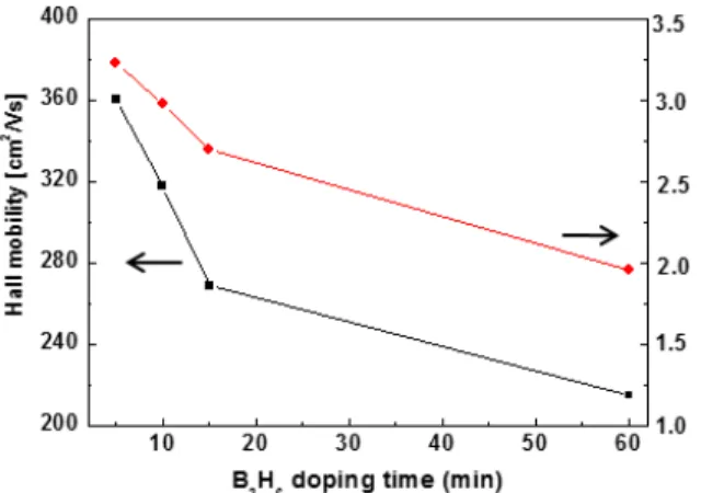
analyzed by the Hall-effect measurements. Fig. 7 shows the mobility and resistivity of the epitaxial poly-Si thin-films as a function of in-situ boron doping time. With an increase in the in-situ boron doping time, the mobility and resistivity decreased.
The highest mobility of 360 cm2/V·s was achieved when the B2H6 gas flow was continued for 5 min and cut off.
We believe that this is due to improved crystallinity of the poly-Si film with a decreasing in-situ boron doping time. When the boron doping time increase, the mobility can be decreased by the intra-grain defects, especially in heavily boron doped Si.
Consequently, high quality poly-Si film was obtained by controlling the in-situ boron doping time.
3.2 Properties of Si thin-film solar cells
Fig. 8 shows a schematic cross section of the Si thin-film solar cell made in our laboratory. The front side consists of a-Si(n)/a-Si(i) layer which is the basic structure of the heterointerface thin (HIT) layer on Si. Our cell is a single-side HIT cell. Boron- doped ZnO (BZO) was used as a transparent conducting oxide.
The back side consists of a poly-Si(p+)/CoSi2 back contact layer.
A CoSi2 layer was used to reduce the sheet resistance of the back electrode. The CoSi2 layer was formed by sputter deposition of Ti/Co/Ti on Si and by annealing at 750°C for 5 min17,18). The sheet resistance of the CoSi2 layer was 100 nm and 2-4 Ω /square, while the sheet resistance of the p+ Si back was more than 60-80 Ω/square without CoSi2. Before applying this structure to thin Si film, a reference with a Si wafer was fabricated and an efficiency of 13.5% cell efficiency was obtained.
Fig. 9 shows the cross sectional image of the Si thin-film solar cell fabricated based on the structure shown in Fig. 8. The CoSi2
layer is clearly seen between the epitaxial Si and the Si substrate.
The thicknesses of BZO, a-Si(n), a-Si(i), p-type Si, p+ Si, and CoSi2 layers were 1000, 30, 30, 1750, 500, and 100 nm, respectively.
Fig. 10 shows the I-V curves (a) and spectral quantum efficiencies (b) with and without the CoSi2 back contact layer, under solar illumination at AM1.5, 100 mW/cm2. The I-V curve of the cell without CoSi2 shows an almost resistive cell. When CoSi2 was used as a back contact, the current density was greatly increased from 3 to 11 mA/cm2 due to lower series resistance.
The efficiency of the cell with a CoSi2 back contact was 0.47%; the short circuit current (Jsc), open circuit voltage (Voc), and fill factor (FF) were 10.4 mA/cm2, 0.142 V, and 0.32, respectively. Even though the efficiency was low, we provide a new approach idea to develop Si thin-film solar cells.
The spectral quantum efficiency (QE) in Fig. 10b shows that current is generated only near the junction region due to a thin depletion layer by high boron doping. The main cause of low efficiency is due to a low Voc. We believe that the doping concentration p-type Si film is too high so that tunneling occurs Fig. 7. Hall mobility and resistivity of the epitaxial poly-Si films
as a function of in-situ boron doping time
Fig. 8. Schematic cross section of the proposed Si thin-film solar cell
Fig. 9. Cross section of the fabricated Si thin-film solar cell
during forward bias. In our experiment, it was difficult to control the boron concentration in the Si. With a lower boron concentration the depletion width can be extended to bulk and the shunt resistance of the a-Si/ploy-Si film heterojunction can be increased, resulting in a larger Voc. Further refinement of our experiment with a sturdier junction can provide higher efficiency.
4. Conclusions
A p-type high-quality crystalline Si film was grown at low 600°C by hot wire CVD using a large-grained poly-Si seed layer. The large-grained poly-Si seed layer was prepared by a VIC process with AlCl3 vapor. The average grain size of the epitaxial poly-Si film was 20 μm. With an increasing boron concentration in the Si film, the quality of the Si film was degraded from the analysis of Raman peak and TEM, indicating more lattice distortion and more defects such as stacking faults.
The boron-doped film had high mobility, but the resistivity was too low. More precise control of doping time was necessary for lower doping. A single-side HIT cell was designed and fabricated using the p-type epitaxial Si film with a CoSi2 back contact. The
short circuit current was greatly improved with the back contact due to a decrease of series resistance. However, the efficiency was much lower than expected mainly due to poor junction by shunt or tunneling due to a high boron doping concentration.
With less B doping the junction will be sturdy and the open circuit voltage will be greatly increased. The results indicated that our approach to growing a thin crystalline Si film with a large-grained seed layer can has a considerable potential for future thin-crystalline Si tin film solar cells.
Acknowledgments
This work was supported by the Engineering Research Center program (2012-0001167) and KAIST EEWS Initiative Program (EEWS-2012-N01120013) funded by Korean Research Foundation, and the Priority Research Center program (2011-0031407) funded by the Korea Ministry of Education.
References
1. M. J. Keevers, T. L. Young, U. Schubert, M. A. Green, in pro- ceedings of the 22nd EU PVSEC, Milan, 1783 (2007).
2. M.A. Green, K. Emery, Y. Hishikawa, and W. Warta, Solar cell efficiency tables (version 43), Prog. Photovoltaics, 22, 1-9 (2014).
3. D. Song, D. Inns, A. Straub, M. L. Terry, P. Campbell, and A.
G. Aberle, Soild phase crystallized polycrystalline thin film on glass from evaporated silicon for photovoltaic applications, Thin Solid Films, 513, 356-363 (2006).
4. I. Gordon, L. Carnel, D. Van Gestel, G. Beaucarne, and J.
Poortmans, 8% efficienct thin-film polycrystalline-silicon solar cells based on aluminum-induced crystallization and thermal CVD, Prog. Photovolt : Res. Appl. 15, 575-586 (2007).
5. D. Van Gestel, I. Gordon, J. Poortmanns, Aluminum-induced crystallization for thin-film polycrystalline silicon solar cells:
achievements and perspectives, Solar Energy Materials & Solar Cells, 119, 261-270 (2013).
6. S. Gall, J. Schneider, J. Klein, K. Hubener, M. Muske, Large-grained polycrystalline silicon on glass for thin-film solar cells, Thin Solid Film, 511, 7-14 (2006).
7. J. H. Eom, K. U. Lee, and B. T. Ahn, A novel vapor-induced crystallization of amorphous Si using the transport of Al/Ni chloride, Electrochem. Solid-State Lett., 8, G65-G67 (2005).
8. K. M. Ahn, S. M. Kang and B. T. Ahn, Fabrication of high-quality polycrystalline silicon film by crystallization of amorphous silicon film using AlCl3 vapor for thin film tran- sistors, J. Electrochem. Soc., 158, H374-H378 (2011).
9. S. M. Kang, K. M, Ahn, and B. T. Ahn, High-quality poly- Fig. 10. Characteristics of the Si thin-film solar cells with and
without CoSi2 back contact
crystalline silicon film crystallized from amorphous silicon film using NiCl2 vapor, J. Electrochem. Soc., 159, H29-H32 (2012).
10. K. M. Ahn, S. M. Kang, S. H. Moon, H. S. Kwon, B. T. Ahn, Low-temperature epitaxial growth of a uniform polycrystalline Si film with large grains on SiO2 substrate by Al-Assisted crystal growth, Current Photovoltaic Research, 1, 103-108 (2013).
11. D. Grozdanic, O. Milat, B. Rakvin, B. Pivac, A. Slaoui, R.
Monna, Grain boundary defects in RTCVD polycrystalline sili- con for solar cells, Vacuum, 61, 257-262 (2001).
12. O. Tuzun, J. M. Auger, I. Gordon, A. Focsa, EBSD analysis of polysilicon films formed by aluminum induced crystallization of amorphous silicon, Thin Solid Film, 516, 6882-6887 (2008).
13. A. Brokman and R. Balluffi, Coincidence lattice model for the structure and energy of grain boundaries, Acta Metall, 29, 1703-1719 (1981).
14. U. Fano, Phys. Rev., 124, 1866 (1961).
15. R. Saleh and N. H. Nickel, The influence of boron concen- trations on structural properties in disorder silicon films, Applied Surface Science, 254, 5800585 (2007).
16. D. J. Eaglesham, Semiconductor molecular-beam epitaxy at low temperatures, J. Appl. Phys., 77(8), 3597-3617 (1995).
17. H. S. Rhee, B. T. Ahn, In situ growth of an epitaxial CoSi2 layer on a Si(100) substrate by reactive chemical-vapor deposition us- ing a cobalt metallorganic source, Appl. Phys. Lett., 21, 3176-3178 (1999).
18. H. S. Lee, H. S. Rhee, B. T. Ahn, Improved morphological sta- bility of CoSi2 layer by in situ growth on polycrystalline silicon using reactive chemical vapor deposition, J. Electrochem. Soc., 149, G16-G20 (2002).


![외국인 PCR검사 가능 기관 [Referral Laboratories : 11sites]](data:image/gif;base64,R0lGODlhAQABAIAAAP///wAAACH5BAEAAAAALAAAAAABAAEAAAICRAEAOw==)