Edge Termination을 위해 Tilt-Implantation을 이용한 SiC Trench Schottky Diode에 대한 연구
A Study of SiC Trench Schottky Diode with Tilt-Implantation for Edge Termination
송 길 용*, 김 광 수*★ Gil-Yong Song*, Kwang-Soo Kim*★
Abstract
In this paper, the usage of tilt-implanted trench Schottky diode(TITSD) based on silicon carbide is proposed.
A tilt-implanted trench termination technique modified for SiC is proposed as a method to keep all the potentials confined in the trench insulator when reverse blocking mode is operated. With the side wall doping concentration of 1x10
19cm
-3nitrogen, the termination area of the TITSD is reduced without any sacrifice in breakdown voltage while potential is confined within insulator. When the trench depth is set to 11um and the width is optimized, a breakdown voltage of 2750V is obtained and termination area is 38.7% smaller than that of other devices which use guard rings for the same breakdown voltage. A Sentaurus device simulator is used to analyze the characteristics of the TITSD. The performance of the TITSD is compared to the conventional trench Schottky diode.
요 약
본 논문에서는 실리콘 카바이드(silicon carbide)를 기반으로 한 tilt-implanted trench Schottky diode(TITSD)를 제 안한다. 4H-SiC 트랜치 쇼트키 다이오드(trench Schottky diode)에 형성되는 트랜치 측면에 경사 이온주입 (tilt-implantation)을 하여 소자가 역저지 상태(reverse blocking mode)로 동작 시 trench insulator가 모든 퍼텐셜 (potential)을 포함하는 구조를 제안하고, 그 특성을 시뮬레이션을 통해 확인하였다. TITSD는 트랜치의 측면(sidewall) 에 nitrogen을 1x10
19cm
-3으로 도밍(doping) 하여 항복전압(breakdown voltage) 특성도 경사 이온주입을 하지 않았을 때와 같게 유지하면서 trench oxide insulator가 모든 퍼텐셜을 포함하도록 함으로써 termination area를 감소시켰다.
트랜치 깊이(trench depth)를 11μm로 깊게 하고 최적화된 폭(width)을 선택함으로써 2750V의 항복전압을 얻었고, 동 급의 항복전압을 가진 가드링(guard ring) 구조보다 termination area를 38.7% 줄일 수 있다. 이에 대한 전기적 특성 은 synopsys사의 TCAD simulation을 사용하여 분석하였으며, 그 결과를 기존의 구조와 비교하였다.
Key words : Silicon Carbide, Schottky Diode, Trench Edge Termination, Tilt Implantation, Power Device
* Dept. of Electronics Engineering, Sogang University
[email protected]010-5435-0032
★
Corresponding author
※ This research was supported by the MSIP(Ministry of Science, ICT and Future Planning), Korea, under the ITRC(Information Technology Research Center)support program(NIPA-2014-H0301-14-1007) supervised by the NIPA(National IT Industry Promotion Agency)
Manuscript received Apr. 29, 2014; revised May. 29, 2014 ; accepted May 29. 2014
Ⅰ. 서론
실리콘 카바이드는 높은 밴드갭(bandgap) 및 임계 전 계(critical electric field), 그리고 높은 열전도성 (thermal conductivity)의 장점을 가지고 있어 전력 반도체 소자에 가장 적합한 물질로 주목받고 있다[1].
고전압으로 많이 사용하는 전력 반도체 소자에서 가 장 중요하게 고려해야 할 전기적 특성은 항복전압과 on-resistance이다. 하지만 쇼트키 다이오드는 Schottky junction edge에서 생기는 전계 집중 (electric field crowding)의 영향 때문에 항복전압이 감소하는 단점이 있다[2]. 이러한 전계 집중을 줄여 항복전압을 높이기 위해 가드링[3], field plate[4], junction termination extension(JTE)[5] 및 field-limited ring[6]과 같은 다양한 방법이 제안되었 다. 하지만 이러한 구조들은 항복전압을 높이기 위해 소자의 면적이 커지는 단점이 있다.
따라서 소자의 크기를 작게 하면서 항복전압을 높이 기 위한 구조로 트랜치 구조를 사용한다. 즉, 실리콘 (silicon)을 기반으로 한 trench termination 구조의 경 우 trench insulator에 field plate를 추가한 뒤 역바이 어스(reverse bias)를 인가하면 측면이 반전 (inversion) 되어 hole이 쌓이게 된다. 이 쌓이게 된 hole 때문에 trench insulator는 퍼텐셜을 insulator 밖
으로 확장하지 못하고 모두 포함하게 되므로
termination area를 줄일 수 있다[7], [8]. 따라서 트랜 치 구조는 작은 면적을 차지하면서 높은 항복전압을 가지는 구조로 많이 사용한다.
하지만 실리콘 카바이드의 경우 진성 캐리어 농도 (intrinsic carrier density)가 5x10
-9cm
-3로 실리콘보다 (1.5x10
10cm
-3) 매우 낮다[1]. 이로 인해 실리콘 트랜치 쇼트키 다이오드가 트랜치 측면이 반전되는 것과 달 리[8], 실리콘 카바이드 트랜치 쇼트키 다이오드는 field plate가 존재하여도 트랜치 측면이 반전 되지 못 하여 hole이 쌓이지 못한다. 따라서 trench insulator 가 모든 퍼텐셜을 포함하지 못하고 밖으로 확장되어 소자의 termination area가 증가한다. 이를 해결하기 위해 본 논문에서는 낮은 진성 캐리어 농도를 가지는 실리콘 카바이드에 특화한 tilt implanted trench Schottky diode(TITSD) 구조를 제안하였다. 제안된 구조는 트랜치 측면에 n dopant를 1x10
19cm
-3의 고농 도로 경사 이온주입을 함으로써 역저지 상태로 동작 시에 항복전압의 변화 없이 퍼텐셜을 trench oxide insulator에 완전히 포함하도록 하였다. 또한, trench
insulator의 깊이와 폭에 따른 항복전압의 변화를 관 찰하여 가드링을 사용한 구조와의 termination area를 비교하였다. 본 논문은 synopsys T-CAD simulation 을 이용하여 분석하였다.
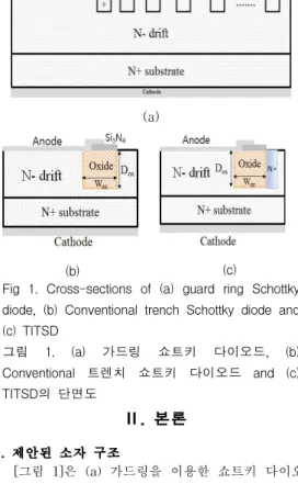
(a)
(b) (c)
Fig 1. Cross-sections of (a) guard ring Schottky diode, (b) Conventional trench Schottky diode and (c) TITSD
그림 1. (a) 가드링 쇼트키 다이오드, (b) Conventional 트렌치 쇼트키 다이오드 and (c) TITSD의 단면도
Ⅱ. 본론
1. 제안된 소자 구조
[그림 1]은 (a) 가드링을 이용한 쇼트키 다이오드 와 (b) conventional 트랜치 쇼트키 다이오드, 그리고 (c) TITSD의 구조를 나타낸다. TITSD는 트랜치 측 면에 경사 이온주입을 이용하여 nitrogen을 고농도로 도핑함으로서 trench oxide insulator가 모든 퍼텐셜을 포함하게 된다. 따라서 가드링 쇼트키 다이오드, conventional 트랜치 쇼트키 다이오드보다 소자의 termination area를 줄일 수 있는 장점이 있다.
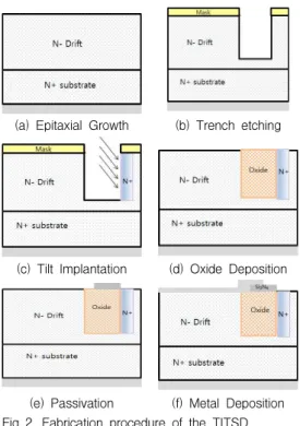
2. 공정순서
[그림 2]는 공정 순서도를 나타낸다. 먼저 4H-SiC
n+기판 위에 1x10
15cm
-3농도로 15μm의 drift region
을 에피 성장(epitaxial growth)를 이용하여 형성한다
[그림 2(a)]. 그 후 식각(etching) 공정을 이용하여 트
랜치할 부분을 형성하고[그림2(b)], 경사 이온주입을
이용하여[그림 2(c)] 측면에 n+를 도핑 한다. 이후에
증착(deposition) 공정을 이용하여 oxide(SiO
2) insulator를 채워 주고 트랜치에 채운 oxide를 제외한 부분을 CMP 공정을 이용하여 제거한다[그림 2(d)].
다음으로 Si
3N
4로 passivation을 시켜준 후에[그림 2(e)], anode metal을 증착 시켜주어 완성한다[그림 2(f)]. 소자의 주요 공정 변수는 Table 1에 나타내었 다. 위 공정은 conventional 트랜치 쇼트키 다이오드 의 구조에서 경사 이온주입을 하는 공정[그림 2(c)]만 이 추가되었다.
(a) Epitaxial Growth (b) Trench etching
(c) Tilt Implantation (d) Oxide Deposition
(e) Passivation (f) Metal Deposition Fig 2. Fabrication procedure of the TITSD 그림 2. TITSD의 공정 순서
Table 1. Process parameters of TITSD and Guard Ring Schottky diode
표 1. TITSD와 guard ring Schottky diode의 주요 공정 변수
변수 TITSD Guard
Ring Epitaxial Width (μm) 15 15
Active (μm) 20 20
Substrate Doping (cm
-3) 1x10
181x10
18Drift Doping (cm
-3) 1x10
151x10
153. 소자 시뮬레이션 결과
[그림 3]은 역바이어스를 인가하였을 때 Si-트랜치 쇼트키 다이오드와 경사 이온주입을 하지 않은 SiC- 트랜치 쇼트키 다이오드의 potential contour를 비교 하였다. [그림 3(a)]로부터 실리콘에 기반을 둔 트랜 치 쇼트키 다이오드는 trench insulator가 모든 퍼텐 셜을 포함하고 있는 것을 확인할 수 있다. 반면에 [그 림 3(b)]로부터 SiC에 기반을 둔 트랜치 쇼트키 다이 오드는 trench insulator가 모든 퍼텐셜을 포함하지 못하고 trench insulator 밖까지 퍼져 나가 있음을 알 수 있다.
(b) (a)
Fig 3. Potential contours of (a) Si trench Schottky diode and (b) SiC-based trench Schottky diode 그림 3. (a) Si 트렌치 쇼트키 다이오드 and (b) SiC 트렌치 쇼트키 다이오드의 potential contour
[그림 4]는 Si에 기반을 둔 트랜치 쇼트키 다이오드 측면에 역바이어스를 인가하였을 때 쌓이는 hole density를 나타낸다. 측면에 쌓이는 hole 때문에 퍼텐 셜이 insulator에 완전히 termination 된다[8]. 따라서 가드링을 사용했을 때보다 termination area를 줄일 수 있는 장점이 있다. 하지만 SiC에 기반을 둔 트랜 치 쇼트키 다이오드의 경우 낮은 진성 캐리어 농도 때문에 field plate가 존재하여도 trench 측면에 hole 이 쌓이지 못하므로 [그림 3(b)]에서 보다시피 trench
Fig 4. Hole density of Si based trench Schottky diode
그림 4. Si 트렌치 쇼트키 다이오드의 hole density
insulator가 퍼텐셜을 포함하지 못한다. 따라서 퍼텐셜 이 퍼지는 정도를 줄이기 위해서 trench 옆에 가드링 과 같은 추가적인 방법이 필요하게 된다.
[그림 5]는 SiC 트랜치 쇼트키 다이오드의 trench 측면에 경사 이온주입을 사용하여 1x10
16cm
-3으로 도 핑 했을 때[그림 5(a)]와 1x10
19cm
-3으로 도핑
(a) (b)
Fig 5. Potential contour as the variation of tilt implantation concentration (a) 1x10
16cm
-3and (b) 1x10
19cm
-3in TITSD
그림 5. TITSD에서 경사 이온주입의 농도에 따른 potential contour (a) 1x10
16cm
-3and (b) 1x10
19cm
-3했을 때의[그림 5(b)] potential contour를 나타낸다.
1x10
16cm
-3으로 경사 이온주입을 해주었을 때도 trench termination이 완벽하게 되지 않았지만, 1x10
19cm
-3으로 경사 이온주입을 하였을 시 trench oxide가 모든 퍼텐셜을 포함하였다.
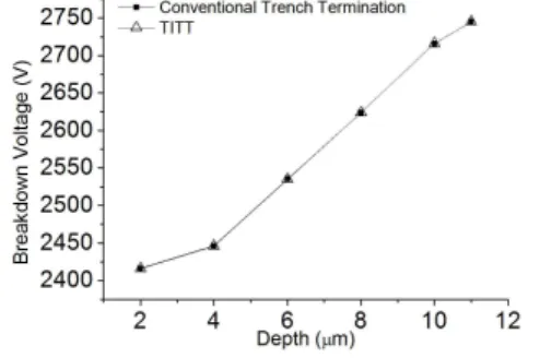
[그림 6]은 TITSD의 trench oxide depth (D
ox)에 따 른 항복전압을 경사 이온주입을 파라미터로 하여 나 타내었다. 트랜치 깊이가 깊어질수록 termination의 영향이 증가하므로 높은 항복전압의의 결과를 얻을 수 있다. 트랜치 깊이를 2μm로 했을 때보다 11μm로
Fig 6. Breakdown voltage as a function of trench depth
그림 6. Trench oxide depth에 따른 항복전압
했을 때 항복전압이 약 13.7% 향상했으며, 경사 이온 주입을 하지 않은 구조와 비교해 보았을 때 같은 값 의 결과가 나왔다. 따라서 항복전압은 유지하면서 trench oxide가 모든 퍼텐셜을 포함한 결과를 얻었다.
[그림 7]은 oxide 깊이에 따른 트랜치의 폭 변화에 따라서 항복전압을 최적화 시킨 값들을 나타내었 다.[9] 항복전압은 oxide 깊이뿐만 아니라 폭에도 영 향을 받음을 알 수 있다. Trench oxide width가 증가 할수록 항복전압이 증가하지만, 14μm 이상으로 증
Fig 7. Breakdown voltage as a function of trench depth with trench width as a parameter 그림 7. Oxide 깊이, 폭에 따른 항복전압
가하면 trench의 효과가 감소하여 항복전압이 더 증 가하지 않는다.
[그림 8]은 가드링 구조와 trench termination 구조의 항복전압을 나타낸다. 가드링의 개수가 6개일 때 2300V급으로 나왔지만, 가드링이 7개 있을 때는 2750V급으로 trench termination과 같은 값을 나타내 었다[3].
Fig 8. 트렌치 쇼트키 다이오드와 가드링 쇼트키 다이오드의 항복전압
그림 8. I-V curves for TITT and Guard rings
structure
[그림 9]는 (a) 가드링이 7개 일 때 쇼트키 다이오드 와 (b) 경사 이온주입을 한 trench termination 쇼트 키 다이오드의 potential contour에 대해 나타내었다.
같은 항복전압을 갖지만, 가드링을 사용한 구조는 potential contour가 62μm까지 확장됐지만 trench termination 구조는 38μm까지만 확장되었음을 확인할 수 있다.
(a) (b)
Fig 9. Potential contour of (a) guard ring Schottky diode and (b) TITSD
그림 9. 가드링 쇼트키 다이오드와 TITSD의 potential contour
[그림 10]은 (a) 가드링 구조와 (b) TITST의 termination area를 나타낸다. 경사 이온주입을 한 트 랜치 쇼트키 다이오드가 가드링 쇼트키 다이오드보다 termination area를 38.7% 감소시킬 수 있다.
(a) (b)
Fig 10. Top view of (a) guad ring Schottky diode and (b) TITSD
그림 10. (a) 가드링 쇼트키 다이오드와 (b) TITSD의 top view
Ⅲ 결론
트랜치 측면에 nitrogen을 경사 이온주입 시켜 줌으 로써 역저지 상태로 동작 시 trench oxide insulator가 모든 퍼텐셜을 포함하는 4H-SiC 트랜치 쇼트키 다이 오드 구조를 simulation을 통해 확인하였다. 제안한 구조는 경사 이온주입을 하지 않은 트랜치 쇼트키 다 이오드보다 측면에 경사 이온주입을 시킨 공정만을 추가하였다. 제안한 소자의 항복전압은 2750V로 계산 되어 경사 이온주입 하지 않은 트랜치 쇼트키 다이오 드 구조와 비교했을 때 항복전압의 감소 없이 potential contour를 trench insulator에 완전히 가둘 수 있었다. 또한, 제안한 구조는 가드링을 사용한 쇼 트키 다이오드보다 termination area를 같은 voltage 급에서 38.7% 감소시켰으며 트랜치 깊이를 11μm로 함으로서 2μm로 하였을 때보다 항복전압이 13.7% 향 상했다. 제안한 구조를 이용함으로써 termination area를 줄일 수 있고, SiC PiN diode 등에도 실리콘 카바이드에 최적화된 trench diode를 구현할 수 있을 것으로 예상한다.
References
[1] B. J. Baliga, “Silicon Carbide Power Devices,” World Scientific, 2005.
[2] B. J. Baliga, “Fundamentals of Power Semi- conductor Devices,” Springer, 2008.
[3] David C. Sherdian, Guofu Niu, J. Neil Merrett, John D. Cressler, Charles Ellis, Chin-Che Tin “Design and Fabrication of Planar Guard Ring Termination for High-voltage SiC Diodes,” Solid-State Electronics, 44, pp. 1367-1372. 2000.
[4] Vik Saxena, Jian Nong Su, Andrew J. Steckl
“High-Voltage Ni- and Pt-SiC Schottky Diodes Utilizing Metal Field Plate Termination,” IEEE Trans, Electron Devices, vol, 46, No. 3, pp. 456-463, March 1999.
[5] Alexander V. Bolotnikov, Peter G. Muzykov, Qungchun, A.K. Agarwal, T. S. Sudarshan “Junction Termination Extension Implementing Drive-in Diffusion of Boron for High-Voltage SiC Devices,”
IEEE Trans. Electron Devices, vol. 57, No.8, pp.
1930-1935, Aug. 2010.
[6] Seong-Jin Kim, Dong-Ju Oh, Soon-Jae Yu,
Yong-Deuk Woo, “Breakdown Voltage Characteristics
of SiC Schottky Barrier Diode of with Aluminum
Deposition Edge Termination Structure,” Journal of
the Korean Physical Society, Vol. 49, pp. S768-S773,
December 2006.
[7] L. Theolier, H. Mahfoz-Kotb, K. Isoird, F. Morancho,
“A New Junction Termination Technique; The Deep Trench Termination (DT
2),” IEEE, pp. 176-179, 2009.
[8] Ryu Kamibaba, Kenichi Takahama, Ichiro Omura
“Design of Trench Termination for High Voltage Devices,” ISPSD, Hiroshima, Japan, pp. 107-110, 2010.
BIOGRAPHY
![그림 9. 가드링 쇼트키 다이오드와 TITSD의 potential contour [그림 10]은 (a) 가드링 구조와 (b) TITST의 termination area를 나타낸다](https://thumb-ap.123doks.com/thumbv2/123dokinfo/4675142.501028/5.772.76.368.665.916/가드링-쇼트키-다이오드와-titsd의-potential-가드링-termination-나타낸다.webp)