유기금속화학기상증착법을 이용한 전이금속 칼코게나이드 단일층 및 이종구조 성장
장수희·신재혁·박원일† 한양대학교 신소재공학과
Metal-organic Chemical Vapor Deposition of Uniform Transition Metal Dichalcogenides Single Layers and Heterostructures
Suhee Jang, Jae Hyeok Shin, and Won Il Park†
Division of Materials Science and Engineering, Hanyang University, Seoul 04763, Republic of Korea (Received December 19, 2020: Corrected December 21, 2020: Accepted December 29, 2020)
초 록: 1.1~2.1eV의 직접 천이형 밴드갭을 가지는 전이금속 칼코게나이드(Transition Metal Dichalcogenide, TMDC) 는 빛에 대한 반응성이 크고 구조적 특징상 2차원 물질들과의 수직 이종접합구조를 형성하기 용이하다는 장점으로 차세 대 광전소자와 반도체소자 물질로서 대두되고 있다. 하지만 TMDC를 얻는 공정들의 한계로 인해 고품질, 대면적의 수직 이종접합구조의 형성에 어려움이 존재한다. 본 연구에서는 MOCVD 시스템을 제작하고, 단일층 TMDC 및 이들의 이종 구조에 제조에 대한 연구를 수행하였다. 특히, 버블러 타입의 유기금속화합물 소스를 활용하여, 반응기 내로 유입되는 소
스의 농도와 유량을 정밀하게 조절함으로써 전면적으로 균일한 박막을 얻을 수 있다. MOCVD로 MoS2, WS2박막을 성
장시키고 주사전자현미경, UV-visible spectrophotometer, Raman spectroscopy, photoluminescence 분석을 진행하여 균일 한 박막을 성장시켰음을 확인하였다. 또한, MoS2박막에 WS2박막을 직접 성장시킴으로써 MoS2/WS2수직 이종접합구 조를 형성하였다.
Abstract: Transition metal dichalcogenides (TMDCs), two-dimensional atomic layered materials with direct bandgap in the range of 1.1-2.1 eV, have attracted a lot of research interest due to their high response to light and capability to build new types of artificial heterostructures. However, the large-area synthesis of high-quality and uniform TMDC films with vertical-stacked heterostructure still remains challenge. In this study, we have developed a metal-organic chemical vapor deposition (MOCVD) system for TMDCs and conducted a systematic study on the growth of single-layer TMDCs and their heterostructures. In particular, using a bubbler-type organometallic compound sources, the concentration and flow rate of each source can be precisely controlled to obtain uniformly single-layered MoS2 and WS2 films over the centimeter scale.
In addition, the MoS2/WS2 vertical heterostructure was achieved by growing WS2 film directly on the MoS2 film, as confirmed by electron microscopy, UV-visible spectrophotometer, Raman spectroscopy, and photoluminescence spectroscopy.
Keywords: TMDC, MOCVD, Vertical heterostructure, MoS2, WS2, two-dimensional material
1. 서 론
플렉서블(flexible), 웨어러블(wearable) 소자와 같은 차 세대 모바일 기술이 중요해 짐에 따라, 유연하고 투명한 2차원 소재들에 대한 연구가 활발히 진행되고 있다. 이러 한 2차원 소재들 중 반금속 물질인 그래핀(graphene),1-5) 반도체 물질인 전이금속 칼코게나이드(transition metal dichalcogenide, TMDC)6,7)와 흑린(black phosphorus),8,9) 절
연체인 육각형질화붕소(hexagonal boron nitration, h-
BN)10-12) 등이 주목 받고 있다.
TMDC는 몰리브데늄(molybdenum, Mo), 텅스텐(tungsten, W)과 같은 6족 전이금속과 황(sulfur, S), 셀레늄(selenium, Se), 텔루륨(tellurium, Te)의 칼코겐 원소로 구성된 세 개 의 원자층이 단일층을 이루고 있는 2차원 반도체 물질이 다. TMDC 물질의 가장 큰 특징은 벌크 상태에서는 간접 천이형(indirect) 밴드갭을 가지지만 단일층의 경우 밴드
†
Corresponding author E-mail: [email protected]
© 2020, The Korean Microelectronics and Packaging Society
This is an Open-Access article distributed under the terms of the Creative Commons Attribution Non-Commercial License(http://creativecommons.org/
licenses/by-nc/3.0) which permits unrestricted non-commercial use, distribution, and reproduction in any medium, provided the original work is
properly cited.
변화가 일어나 1.1~2.1 eV의 직접 천이형(direct) 밴드갭을 가진다는 것이다.6) 또한 결합력이 강한 엑시톤을 형성함 으로써 빛에 대한 강한 반응성을 나타낸다.7) TMDC 물질 은 구조적으로 안정적이고 반응성이 적은 표면을 가지고 있으며, 층 간에 반데르발스 힘(van der Waals force)에 의 해 적층되기 때문에 같은 TMDC 뿐만 아니라 다른 2차 원 물질들과도 쉽게 수직 이종접합구조를 형성할 수 있 다. 또한 그 과정에서 발생하는 격자불일치에 의한 스트 레인(strain)을 최소화 할 수 있다는 장점이 있다. 2차원 수직 이종접합구조 형성 시 구성물질 각각의 고유한 특 성은 물론 전혀 새로운 효과를 얻을 수 있어 관련 연구가 많이 진행되고 있다.13-18)
하지만 현재 TMDC의 수직 이종접합구조를 형성하는 연구에 어려움이 존재한다. 폭넓은 응용을 위해서는 고 품질, 대면적의 수직 이종접합 박막을 얻어야 하지만 단 일층의 TMDC 박막을 합성하는 방법에 있어 한계가 존 재한다. TMDC 박막을 얻는 방법에는 크게 물리/화학적 박리법(mechanical/chemical exfoliation),19-21) 화학기상 증착법(chemical vapor deposition, CVD),22-25) 마그네트 론 스퍼터링(magnetron sputtering),26-28) 분자빔 에피택시 (molecular beam epitaxy, MBE),29-31) 유기화학기상증착법 (metal-organic chemical vapor deposition, MOCVD),32-36) 원 자층증착법(atomic layer deposition, ALD)37-39)이 많이 사 용되고 있다. 대표적으로, 박리법은 벌크 상태의 TMDC 물질로부터 물리/화학적인 힘으로 박막을 분리해내는 방 법으로, 과정이 간단하고 고품위 시편을 얻는데 유리하 다. 하지만, 대면적으로 균일한 박막을 얻기 힘든 단점이 있다. 한편, CVD 기반의 TMDC 성장에서는 주로 고체 형태의 소스(예, Mo 파우더)를 가열하여 기화시킨 후 반 응기 내의 기판에서 박막 형성을 유도한다. CVD법을 이 용하면 원칙적으로 대면적 성장이 가능하지만, 열에 의 해 발생한 소스 vapor를 이용하기 때문에 소스의 농도를 독립적으로 정밀하게 조절할 수 없다는 한계가 있다. 이
에 반해 MOCVD 성장법에서는 고체 소스 대신에 유기 금속화합물 형태(예, Mo(CO)6)의 소스를 사용한다. 특히, 버블러(bubbler) 등에 유기금속화합물 소스를 넣고, Ar, N2 등의 캐리어(carrier) 가스를 일정한 속도로 흘려주면 서 반응기 내로 유입되는 소스의 농도와 유량을 정밀하 게 제어할 수 있다는 장점이 있고 이종 소재의 합성에도 유리하다.
본 연구에서는 TMDC 합성을 위한 버블러 타입의 MOCVD를 직접 제작하고 이황화몰리브덴(Molybdenum Disulfide, MoS2), 이황화텅스텐(Tungsten Disulfide, WS2) 박막 형성을 진행하였다. 성장된 박막 소재에 대해, 주사 현미경(scanning electron microscope, SEM), UV-visible spectrophotometer, photoluminescence (PL), Raman spec- troscopy 분석을 통해 센티미터 크기의 균일한 단일층의 박막이 합성되었음을 확인하였다. 또한, 단일층 MoS2 위 에 WS2단일층을 직접 성장시킴으로써 수직 이종접합 소 재의 형성을 확인하였다.
2. 실험 방법 2.1. TMDC 성장을 위한 MOCVD 셋업
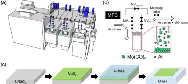
고품질의 균일한 TMDC 박막을 합성하기 위해 버블러 타입의 MOCVD 시스템을 직접 제작하였다. Fig. 1(a)는 본 연구실에서 제작한 MOCVD의 모식도이다. 모식도의 왼쪽 파트는 성장이 일어나는 가열로와 내경이 2 inch인 쿼츠 튜브로 구성된 반응기를 나타낸다. 오른쪽 파트는 대표적인 TMDC 소재의 구성 원소인 Mo, W, S 등의 MO 소스가 각각 들어있는 버블러와 항온조, Ar 캐리어를 위 한 유량제어기(mass flow controller, MFC) 등으로 구성된 가스 라인이다. Mo, W, S 소스로는 각각 molybdenum hexacarbonyl (Mo(CO)6, MHC, Sigma-Aldrich), tungsten hexacarbonyl (W(CO)6, THC, Sigma-Aldrich), diethyl sulfide ((C2H5)2S, DES, Sigma-Aldrich)를 사용하였다.
Fig. 1. (a) 3D scheme of MOCVD system. (b) 2D scheme of bubbler and gas lines. (c) Scheme of MoS2 thin film growth and wet transfer.
Fig. 1(b)는 버블러 부분을 모식도로 나타낸 것으로, 항 온조로 버블러 내부의 온도를 일정하게 유지해주고, 버 블러 자체로 내부 압력을 일정하게 유지할 수 있다. 이를 통해 Ar 대비 MO 소스의 비율을 항상 일정하게 유지할 수 있고, 합성 시 버블러로 유입되는 Ar 캐리어 가스를 정밀하게 조절함으로써 반응에 참여하는 소스의 양을 미 세하게 조절할 수 있다.
2.2. TMDC 박막 합성
성장되는 TMDC 박막의 품질을 높이기 위해서 Si/SiO2
기판을 아세톤(acetone) 용액에 담근 후 5분 동안 초음파 세척 처리를 해주고, 아세톤에 의한 잔여물을 제거하기 위해 이소프로필 알코올(isopropanol alcohol, IPA)와 탈이 온수(DI water)로 세척한다. 그 후, TMDC를 MOCVD법 을 이용해서 600oC에서 18시간동안 성장시켜준다. 합성 과정 중 MOCVD는 Ar (100 sccm), H2 (10 sccm) 분위기 로 5 torr를 유지하며, Ar 가스를 캐리어 가스로 사용하여 각각 버블러의 소스를 일정 속도(Mo/W: 4 sccm, S: 2 sccm)로 공급하여 균일한 박막을 합성한다.
2.3. TMDC 박막의 전사
MOCVD법으로 합성한 TMDC 박막을 슬라이드글라스 로 전사하기 위해, PMMA (Poly Methyl Methacrylate, C4) 를 사용한 습식전사법을 이용하였다. Fig. 1(c)와 같이 PMMA를 스핀코팅(spin-coating)으로 Si/SiO2/MoS2위에 균일하게 코팅해준 후 1:10 비율로 희석한 HF 수용액에 띄워주면 SiO2 층이 녹아 PMMA/MoS2 층만 분리된다. 이 를 DI water에 옮기고 슬라이드 글라스로 알맞은 위치에 뜨면 쉽게 전사가 가능하다. 이때, 75oC 오븐에서 10분간
건조 과정을 거치면 TMDC 박막과 기판과의 접착이 견 고해진다. 또한, PMMA 코팅층은 아세톤 용액에 15분 담 그는 것으로 쉽게 제거 가능하다. 마지막으로, 아세톤 용 액의 잔여물을 제거하기 위해 IPA, DI water 순으로 세척 과정을 진행한다.
2.4. TMDC 박막의 분석
TMDC 박막의 표면을 관찰은 FE-SEM(JSM-7600, JEOL Ltd.)을 사용해 수행하였다. TMDC 박막이 한 층으 로 성장된 것을 확인하기 위해 투과도(UV-ViS, Lambda 650S), Raman과 PL(532 nm laser/CCD camera: iDus 420, DV420A-OE)을 사용하였다.
3. 결과 및 고찰
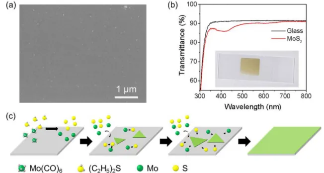
균일한 단일층의 TMDC 박막을 합성하기 위해서는 MOCVD법을 이용해 정밀하게 소스 량을 조절하는 것이 필수이다. 이를 통해 단일층의 박막이 형성되기 전에는 두 층을 형성하지 않는 성장 매커니즘인 ‘self-limited- growth’를 가능하게 한다.34) Fig. 2(c)는 self-limited-growth 에 의해 MoS2 박막이 합성되는 과정을 나타낸 모식도이 다. 첫 번째 단계는 metal-organic 상태로 존재하는 MHC 와 DES가 분해되는 과정이다. MHC는 400oC 이상에서 열분해가 일어나고, DES는 H2에의한 환원반응이 일어나 각각 Mo와 S 원자만 남게 된다. 이때 MO 소스가 모두 분해되는 온도에서 합성이 일어나야 소스의 양을 정밀하 게 조절할 수 있다. 두 번째 단계는 Mo, S 원자들이 기판 에 흡착하고 이동하여 flake를 형성하는 과정이다. 세 번 째 단계는 흡착한 원자들이 이동하여 기존 flake의 edge
Fig. 2. (a) SEM image of MoS2 thin film. (b) Transmittance spectra of glass (reference, black) and MoS2 thin film (red). Inset image shows MoS2 thin film transferred on glass. (c) Schematic illustrating the self-limited-growth of MoS2 film.
에 달라붙어 flake가 성장하는 과정이다. 이 때 self-limited- growth에 의해 기존 flake의 면 위에 흡착된 원자들도 해 당 flake의 edge로 이동한 후 달라붙음으로써 마지막 그 림과 같이 균일한 단일층의 박막을 합성할 수 있다.
MOCVD 공정을 통해 1 cm × 1 cm의 균일한 단일층 의 MoS2 박막을 성장시켰고 SEM, Raman spectroscopy 등의 광학적 분석으로 그 특성을 확인하였다. Fig. 2(a) 의 SEM 사진을 보면 전체 면적에서 균일한 표면을 확 인할 수 있다. Fig. 2(b) 그래프 아래의 사진은 성장시 킨 MoS2 박막을 슬라이드 글라스에 전사한 후의 사진 이고, 그래프는 그 투과도(transmittance)를 측정한 것으 로서, 단일층의 MoS2 박막이 균일하게 성장되었음을 알 수 있다.
TMDC 물질은 Raman spectroscopy 분석을 진행하면 특
징적으로 A1g와 E12g 두 픽(peak)이 나타나는데, A1g 픽은 원자의 out-of-plane 진동에 의해 나타나는 픽이고, E12g은 원자의 in-plane 진동에 의해 나타나는 픽이다.40,41) 특히 MoS2는 380 cm−1에서 410 cm−1 사이에 나타나는 두 픽 사 이의 간격이 벌크 상태에서 단일층으로 갈수록 좁아진다 는 특징이 있어 얇은 MoS2 박막의 층 수의 확인이 가능 하다. 본 연구에서 성장시킨 MoS2박막을 532 nm 파장의 레이저를 사용하는 Raman spectroscopy로 측정한 그래프 를 보면, 두 픽 사이의 간격이 20.62 cm−1로서, 단일층의 박막임을 확인할 수 있다(Fig. 3(a)).
TMDC는 단일층일 경우에만 강한 PL 특성을 나타내기 때문에, PL 픽의 세기와 위치를 측정하는 것이 TMDC가 단일층임을 알 수 있는 효과적인 방법 중 하나이다. Fig.
3(b) 그래프를 보면, 1.88 eV에서 나타나는 강한 PL 픽을
Fig. 3. (a) Typical Raman and (b) PL spectra of single layer MoS2 film. (c) Raman spectra measured at 4 different places on 1cm?1cm MoS2 thin film (inset).
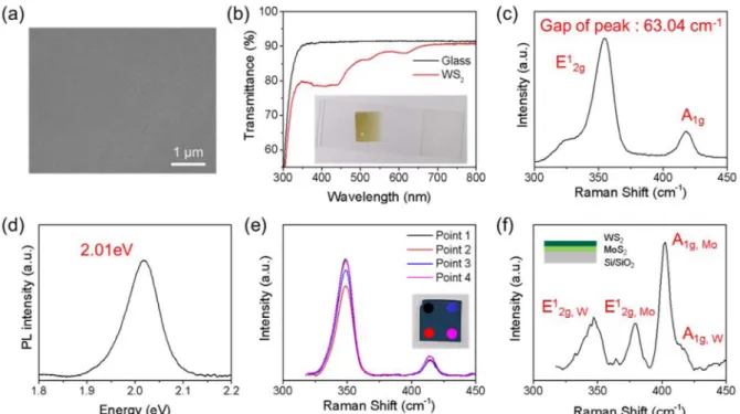
Fig. 4. (a) SEM image of WS2 thin film (b) Transmittance spectra of glass (reference, black) and WS2 thin film (red). Inset: WS2 thin film on glass. (c) Raman and (d) PL spectra of single layer WS2 film. (e) Raman spectra at 4 different places on 1cm?1cm WS2 thin film (inset). (f) Raman spectra of vertically stacked MoS2/WS2 heterostructure. Inset: cross sectional structure of the MoS2/ WS2 heterostructure.
관찰할 수 있었고, 이를 통해 MOCVD를 이용해 성장시 킨 MoS2가 단일층임을 확인 할 수 있다.
본 연구에서 성장시킨 MoS2 박막이 단일층으로 균일 하게 성장되었는지 확인하기 위해 1 cm × 1 cm 샘플의 네 부분의 Raman 측정을 진행하였다. 그 결과, Fig. 3(c)의 그래프와 같이 A1g와 E12g 픽 사이의 간격이 네 지점 모두 Fig. 3(a)와 동일한 것을 확인하였다.
본 연구에서는 MoS2 뿐만 아니라 다른 종류의 TMDC 물질인 WS2도 MOCVD를 이용해 단일층의 균일한 박막 합성이 가능함을 보이고, MoS2/WS2 수직 이종접합 박막 을 직접적으로 성장시킬 수 있음을 확인하였다. Fig. 4(a) 의 SEM 사진과 Fig. 4(b)의 투과도 그래프를 보면, 단일 층의 균일한 WS2 박막을 확인할 수 있다.
WS2의 경우에도 MoS2와 마찬가지로 A1g와 E12g두 픽 이 나타나지만, 두 픽 사이의 간격보다는 E12g 픽의 세기 에 대한 A1g픽의 세기의 비율을 통해 층수를 판별할 수 있다.42) 그 비율이 1 이하인 경우에 WS2가 단일층으로 판단할 수 있다. Fig. 4(c) 그래프는 본 연구에서 MOCVD 를 이용해 합성한 WS2 박막을 Raman spectroscopy로 분 석한 것으로서, E12g 픽에 대한 A1g 픽 세기의 비율이 약 0.26으로 1보다 작은 것을 관찰하였다. 이를 통해 성장 시킨 WS2 박막이 단일층임을 확인할 수 있다. 또한, Fig.
4(d)의 PL 그래프에서 2.01 eV의 강한 PL 픽을 통해서도 단일층의 WS2 박막이 성장되었음을 알 수 있다. Fig. 4(e) 의 그래프를 보면, 1 cm × 1 cm WS2박막의 네 부분을 Raman 분석한 것으로, 네 부분에서 모두 E12g 픽에 대한 A1g 픽 세기 비율이 1 미만인 것이 관찰되었다. 이를 통 해 균일한 단일층의 WS2 박막을 함성하였음을 확인할 수 있다.
MoS2, WS2각각의 박막뿐만 아니라 MoS2/WS2수직 이종접합 박막을 MOCVD 시스템을 이용해 직접 합성 하였다. MoS2박막을 동일 조건으로 먼저 성장시킨 후, 그 위에 WS2 박막 성장 조건으로 WS2를 성장시킴으로 써 균일한 수직 이종접합 박막을 직접 합성할 수 있다.
Fig. 4(f)의 그래프에서 MoS2와 WS2의 라만 픽을 모두 명확히 관찰할 수 있다. 또한, MoS2는 두 픽 사이의 간 격이 22.49 cm−1, WS2는 두 픽 세기의 비율이 약 0.44로 증가한 것을 통해 MoS2와 WS2 두 물질의 합금 형태의 합성이 아닌 MoS2, WS2 각각의 두 박막이 반데르발스 힘으로 수직 이종접합을 이루는 형태로 성장되었음을 확 인할 수 있다.
4. 결 론
본 연구에서는, 버블러 타입의 MOCVD를 제작하여 MoS2와 WS2 박막을 성장시켰고 SEM, Raman spectro- scopy 등의 표면, 광학 분석을 통해 균일한 단일층의 박 막임을 확인하였다. MOCVD를 이용하는 경우 가열로 로 유입되는 소스의 유량을 정밀하게 조절할 수 있어
TMDC 박막의 성장제어에 용이하다. 나아가, MoS2 박 막 위에 WS2 박막을 직접 성장시킴으로써 MoS2/WS2
반데르발스 힘에 의한 수직 이종접합구조를 형성하였 다. 이를 통하여, 기존의 2차원 소재들간의 수직 이종접 합을 형성하는 과정에서 발생하는 문제점들을 최소화 할 수 있으며, 향후 2D photo-transistor, semiconductor device, photo-detector 등의 2차원 소재 이종접합구조의 활용 범위와 그 특성 향상을 가져올 수 있을 것이라 기 대된다.
References
1. S. H. Kim, J. Jiang, S. Jang, J. H. Lee, D. W. Yang, W. J.
Chang, J. H. Shin, N. Oh, J. Kim, R. Pachter, and W. I. Park,
“Fast synthesis of large-scale single-crystal graphene with well-defined edges upon sodium chloride addition”, Carbon, 158, 904 (2020).
2. S. H. Kim, J. H. Lee, J. S. Park, M. S. Hwang, H. G. Park, K. J. Choi, and W. I. Park, “Performance optimization in gate- tunable Schottky junction solar cells with a light transparent and electric-field permeable graphene mesh on n-Si”, Journal of Materials Chemistry C, 5, 3183 (2017).
3. J. H. Shin, S. H. Kim, S. S. Kwon, and W. I. Park, “Direct CVD growth of graphene on three-dimensionally-shaped dielectric substrates”, Carbon, 129, 785 (2018).
4. S. W. Bang, H. K. Rho, H. J. Bae, S. J. Kang, and J. S. Ha,
“Improvement of electrochemical reduction characteristics of carbon dioxide at porous copper electrode using graphene”, J. Microelectron. Packag. Soc., 25(4), 105 (2018).
5. J. H. Lee, J. H. Shin, S. I. Lee, and W. I. Park, “Review on electric-field transparent conduct electrodes based on nano- materials”, J. Microelectron. Packag. Soc., 27(1), 9 (2020).
6. J. Kang, S. Tongay, J. Zhou, J. B. Li, and J. Q. Wu, “Band offsets and heterostructures of two-dimensional semiconduc- tors”, Appl. Phys. Lett., 102(1), 012111 (2013).
7. J. Li, Y. L. Zhong, and D. Zhang, “Excitons in monolayer transition metal dichalcogenides”, Journal of Physics: Con- densed Matter, 27(31), 315301 (2015).
8. M. M. Luo, T. J. Fan, Y. Zhou, H. Zhang, and L. Mei, “2D Black Phosphorus-Based Biomedical Applications”, Advanced Functional Materials, 29(13), 1808306 (2019).
9. J. L. Zhao, J. J. Zhu, R. Cao, H. D. Wang, Z. N. Guo, D. K.
Sang, J. N. Tang, D. Y. Fan, J. Q. Li, and H. Zhang, “Liq- uefaction of water on the surface of anisotropic two-dimen- sional atomic layered black phosphorus”, Nature communications, 10(1), 1 (2019).
10. M. J. Cui, S. M. Ren, J. Chen, S. Liu, G. G. Zhang, H. C.
Zhao, L. P. Wang & Q. J. Xue, “Anticorrosive performance of waterborne epoxy coatings containing water-dispersible hexagonal boron nitride (h-BN) nanosheets”, Appl Surf Sci, 397, 77-86 (2017).
11. R. Kumar, S. Sahoo, E. Joanni, R. K. Singh, R. M. Yadav, R. K. Verma, D. P. Singh, W. K. Tan, A. P. del Pino, S. A.
Moshkalev, and A. Matsuda, “A review on synthesis of graphene, h-BN and MoS2 for energy storage applications:
Recent progress and perspectives”, Nano Research, 12, 2655 (2019).
12. R. Z. Wang, D. G. Purdie, Y. Fan, F. C. P. Massabuau, P. Brae- uninger-Weimer, O. J. Burton, R. Blurne, R. Schloegl, A.
Lombardo, R. S. Weatherup, and S. Hofmann, “A Peeling Approach for Integrated Manufacturing of Large Monolayer h-BN Crystals”, Acs Nano, 13, 2114 (2019).
13. A. Avsar, J. Y. Tan, X. Luo, K. H. Khoo, Y. T. Yeo, K. Wata- nabe, T. Taniguchi, S. Y. Quek, and B. Ozyilmaz, “van der Waals Bonded Co/h-BN Contacts to Ultrathin Black Phos- phorus Devices”, Nano Lett., 17, 5361 (2017).
14. H. A. Chen, W. C. Chen, H. Sun, C. C. Lin, and S. Y. Lin,
“Scalable MoS2/graphene hetero-structures grown epitaxially on sapphire substrates for phototransistor applications”, Semi- conductor Science and Technology, 33(2), 025007 (2018).
15. J. Ji, C. M. Delehey, D. N. Houpt, M. K. Heighway, T. Lee, and J. H. Choi, “Selective Chemical Modulation of Interlayer Excitons in Atomically Thin Heterostructures”, Nano Lett., 20(4), 2500 (2020).
16. G. H. Shin, C. Park, K. J. Lee, H. J. Jin, and S. Y. Choi,
“Ultrasensitive Phototransistor Based on WSe2-MoS2 van der Waals Heterojunction”, Nano Lett., 20(8), 5741 (2020).
17. J. G. Wang, F. C. Ma, W. J. Liang, and M. T. Sun, “Electrical properties and applications of graphene, hexagonal boron nitride (h-BN), and graphene/h-BN heterostructures”, Mate- rials Today Physics, 2, 6 (2017).
18. X. R. Zong, H. M. Hu, G. Ouyang, J. W. Wang, R. Shi, L.
Zhang, Q. S. Zeng, C. Zhu, S. H. Chen, C. Cheng, B. Wang, H. Zhang, Z. Liu, W. Huang, T. H. Wang, L. Wang, and X.
L. Chen, “Black phosphorus-based van der Waals heterostruc- tures for mid-infrared light-emission applications”, Light: Sci- ence & Applications, 9(1), 1 (2020).
19. S. Bertolazzi, J. Brivio, and A. Kis, “Stretching and Breaking of Ultrathin MoS2”, ACS Nano, 5(12), 9703 (2011).
20. C. X. Huo, Z. Yan, X. F. Song, and H. B. Zeng, “2D materials via liquid exfoliation: a review on fabrication and applica- tions”, Science bulletin, 60(23), 1994 (2015).
21. N. D. Mansukhani, L. M. Guiney, P. J. Kim, Y. C. Zhao, D.
Alducin, A. Ponce, E. Larios, M. J. Yacaman, and M. C. Her- sam, “High-Concentration Aqueous Dispersions of Nanoscale 2D Materials Using Nonionic, Biocompatible Block Copoly- mers”, Small, 12(3), 294 (2016).
22. S. W. Jung, S. Pak, S. Lee, S. Reimers, S. Mukherjee, P.
Dudin, T. K. Kim, M. Cattelan, N. Fox, S. S. Dhesi, C. Cacho, and S. Cha, “Spectral functions of CVD grown MoS2 mono- layers after chemical transfer onto Au surface”, Appl. Surf.
Sci., 532, 147390 (2020).
23. T. Y. Kim, Y. Song, K. Cho, M. Amani, G. H. Ahn, J. K. Kim, J. Pak, S. Chung, A. Javey, and T. Lee, “Analysis of the inter- face characteristics of CVD-grown monolayer MoS2 by noise measurements”, Nanotechnology, 28(14), 145702 (2017).
24. A. A. Koos, P. Vancso, M. Szendro, G. Dobrik, D. A. Silva, Z.
I. Popov, P. B. Sorokin, L. Henrard, C. Y. Hwang, L. P. Biro, and L. Tapaszto, “Influence of Native Defects on the Elec- tronic and Magnetic Properties of CVD Grown MoSe2 Single Layers”, The Journal of Physical Chemistry C, 123(40), 24855 (2019).
25. G. U. Ozkucuk, C. Odaci, E. Sahin, F. Ay, and N. K. Perkgoz,
“Glass-assisted CVD growth of large-area MoS2, WS2 and MoSe2 monolayers on Si/SiO2 substrate”, Materials Science in Semiconductor Processing, 105, 104679 (2020).
26. M. K. S. Bin Rafiq, N. Amin, H. F. Alharbi, M. Luqman, A.
Ayob, Y. S. Alharthi, N. H. Alharthi, B. Bais, and M. Akhta- ruzzaman, “WS2: A New Window Layer Material for Solar Cell Application”, Scientific Reports (Nature Publisher Group), 10(1), 1 (2020).
27. A. Karatas and M. Yilmaz, “Molybdenum disulfide thin films fabrication from multi-phase molybdenum oxide using mag- netron sputtering and CVD systems together”, Superlattices and Microstructures, 143, 106555 (2020).
28. Y. X. Zhang, Y. H. Wang, Z. Z. Xiong, H. J. Zhang, and F.
Liang, “Preparation and characterization of WSe2 nano-films by magnetron sputtering and vacuum selenization”, Nano- technology, 29(27), 275201 (2018).
29. H. C. Diaz, Y. J. Ma, R. Chaghi, and M. Batzill, “High density of (pseudo) periodic twin-grain boundaries in molecular beam epitaxy-grown van der Waals heterostructure: MoTe2/MoS2”, Applied Physics Letters, 108(19), 191606 (2016).
30. Y. Y. Yu, G. Wang, S. Q. Qin, N. N. Wu, Z. Y. Wang, K. He, and X. A. Zhang, “Molecular beam epitaxy growth of atom- ically ultrathin MoTe2 lateral heterophase homojunctions on graphene substrates”, Carbon, 115, 526 (2017).
31. Y. Zhang, T. R. Chang, B. Zhou, Y. T. Cui, H. Yan, Z. K. Liu, F. Schmitt, J. Lee, R. Moore, Y. L. Chen, H. Lin, H. T. Jeng, S. K. Mo, Z. Hussain, A. Bansil, and Z. X. Shen, “Direct observation of the transition from indirect to direct bandgap in atomically thin epitaxial MoSe2”, Nature Nanotechnology, 9(2), 111 (2014).
32. D. Andrzejewski, H. Myja, M. Heuken, A. Grundmann, H.
Kalisch, A. Vescan, T. Kummell, and G. Bacher, ‘Scalable Large-Area p-i-n Light-Emitting Diodes Based on WS2 Monolayers Grown via MOCVD”, Acs Photonics, 6(8), 1832 (2019).
33. S. M. Eichfeld, L. Hossain, Y. C. Lin, A. F. Piasecki, B. Kupp, A. G. Birdwell, R. A. Burke, N. Lu, X. Peng, J. Li, A. Azcatl, S. McDonnell, R. M. Wallace, M. J. Kim, T. S. Mayer, J. M.
Redwing, and J. A. Robinson, “Highly Scalable, Atomically Thin WSe2 Grown via Metal-Organic Chemical Vapor Depo- sition”, Acs Nano, 9(2), 2080 (2015).
34. K. Kang, S. E. Xie, L. J. Huang, Y. M. Han, P. Y. Huang, K. F. Mak, C. J. Kim, D. Muller, and J. Park, “High-mobility three-atom-thick semiconducting films with wafer-scale homogeneity”, Nature, 520(7549), 656 (2015).
35. Y. C. Lin, R. K. Ghosh, R. Addou, N. Lu, S. M. Eichfeld, H. Zhu, M. Y. Li, X. Peng, M. J. Kim, L. J. Li, R. M. Wallace, S. Datta, and J. A. Robinson, “Atomically thin resonant tunnel diodes built from synthetic van der Waals heterostructures”, Nat. Commun., 6(1), 1 (2015).
36. M. Marx, A. Grundmann, Y. R. Lin, D. Andrzejewski, T.
Kummell, G. Bacher, M. Heuken, H. Kalisch, and A. Vescan,
“Metalorganic Vapor-Phase Epitaxy Growth Parameters for Two-Dimensional MoS2”, J. Electron. Mater., 47(2), 910 (2018).
37. J. J. Pyeon, S. H. Kim, D. S. Jeong, S. H. Baek, C. Y. Kang, J. S. Kim, and S. K. Kim, “Wafer-scale growth of MoS2 thin films by atomic layer deposition”, Nanoscale, 8(20), 10792 (2016).
38. L. K. Tan, B. Liu, J. H. Teng, S. F. Guo, H. Y. Low, H. R.
Tan, C. Y. T. Chong, R. B. Yang, and K. P. Loh, “Atomic layer deposition of a MoS2 film”, Nanoscale, 6(18), 10584 (2014).
39. S. Yeo, D. K. Nandi, R. Rahul, T. H. Kim, B. Shong, Y. Jang,
J. S. Bae, J. W. Han, S. H. Kim, and H. Kim, “Low-tempera- ture direct synthesis of high quality WS2 thin films by plasma-enhanced atomic layer deposition for energy related applications”, Appl. Surf. Sci., 459, 596 (2018).
40. H. Li, Q. Zhang, C. C. R. Yap, B. K. Tay, T. H. T. Edwin, A. Olivier, and D. Baillargeat, “From Bulk to Monolayer MoS2: Evolution of Raman Scattering”, Adv. Funct. Mater., 22(7), 1385 (2012).
41. A. G. Bagnall, W. Y. Liang, E. A. Marseglia, and B. Welber,
“Raman Studies of Mos2 at High-Pressure”, Physica B+C, 99, 343 (1980).
42. A. Berkdemir, H. R. Gutierrez, A. R. Botello-Mendez, N.
Perea-Lopez, A. L. Elias, C. I. Chia, B. Wang, V. H. Crespi, F. Lopez-Urias, J. C. Charlier, H. Terrones, and M. Terrones,
“Identification of individual and few layers of WS2 using Raman Spectroscopy”, Scientific reports, 3(1), 8 (2013).