• 검색 결과가 없습니다.

Fabrication and Vibration Characterization of a Partially Etched-type Artificial Basilar Membrane

N/A
N/A
Protected

Academic year: 2021

Share "Fabrication and Vibration Characterization of a Partially Etched-type Artificial Basilar Membrane"

Copied!
6
0
0

로드 중.... (전체 텍스트 보기)

전체 글

(1)

http://dx.doi.org/10.5369/JSST.2015.24.6.373 pISSN 1225-5475/eISSN 2093-7563

Fabrication and Vibration Characterization of a Partially Etched-type Artificial Basilar Membrane

Hanmi Kang

1,2

, Youngdo Jung

1

, Jun-Hyuk Kwak

1

, Kyungjun Song

1

, Seong Ho Kong

2,+

, and Shin Hur

1,+

Abstract

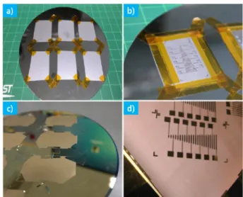
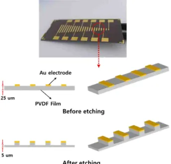
The structure of the human ear is divided into the outer ear, the middle ear, and the inner ear. The inner ear includes the cochlea that plays a very important role in hearing. Recently, the development of an artificial cochlear device for the hearing impaired with cochlear damage has been actively researched. Research has been carried out on the biomimetic piezoelectric thin film ABM (Artificial Basilar Membrane) in particular. In an effort to improve the frequency separation performance of the existing piezoelectric thin film ABM, this paper presents the design, fabrication, and characterization of the production and performance of a partially etched-type ABM material.

O

2

plasma etching equipment was used to partially etch a piezoelectric thin film ABM to make it more flexible. The mechanical-behav- ior characterization of the manufactured partially etched-type ABM showed that the overall separation frequency range shifted to a lower frequency range more suitable for audible frequency bandwidths and it displayed an improved frequency separation performance. In addition, the maximum magnitude of the vibration displacement at the first local resonant frequency was enhanced by three times from 38 nm to 112 nm. It is expected that the newly designed, partially etched-type ABM will improve the issue of cross-talk between nearby electrodes and that the manufactured partially etched-type ABM will be utilized for next-generation ABM research.

Keywords: PVDF film, PVDF sensor, ABM (Artificial Basilar Membrane), O

2

plasma etching

1. INTRODUCTION

The human ear structure (Fig. 1) is made up of the outer ear, the middle ear, and the inner ear. When external sound occurs, the pinna that is part of the outer ear is used to gather the sound and it is then sent to the eardrum via the external canal. The eardrum vibrates in response to the delivered sound that is then mechanically amplified by three small bones in the middle ear called the ossicles, connected to the eardrum, and sent to the inner ear. The inner ear includes the cochlea, an important organ that converts vibration into electrical signals. The vibration of the received sound is separated according to its frequency by the basilar membrane inside the cochlea and the hair cells beneath the

basilar membrane react to its movement generating electrical signals. The generated electrical signals are transmitted to the auditory nerve and this stimulation is sent to the cerebrum to recognize the sound [1-3]. Recently, there has been a marked increase in the number of hearing impaired in Korea receiving cochlear implantations.

Cochlear implantation is performed for patients having hearing disabilities that cannot be corrected with hearing aids, owing to abnormalities in the cochlea of the inner ear or a dysfunctional auditory nervous system [4,5]. The components of the artificial cochlea can be divided into an external and an internal device. The external device comprises a microphone, a speech processor, a transmitter, and a battery, whereas the internal device is made up of a receiver antenna and electrodes that are implanted in the body. To explain the operating principle of the artificial cochlea in simple terms, the various sounds outside are detected by a microphone and converted into electrical signals. These signals are sent to a speech processor and transformed into stimuli according to the signal characteristics. The stimuli are transmitted to the electrodes via a transmitter-receiver. The electrodes stimulate the auditory nerves corresponding to a specific location according to the sent signals, and this stimulation is sent to the cerebrum. Artificial cochlea that have been developed up till now have certain disadvantages including a feeling of discrimination

1

Department of Nature-Inspired Nano Convergence System, Korea Institute of Machinery and Materials, Daejeon, Korea

156 Gajeongbuk-Ro, Yuseong-gu, Daejeon, 305-343, Korea

2

School of Electronics Engineering, Kyungpook National University, Daegu, Korea

80 Daehakro, Bukgu, Daegu, 702-701, Korea

+

Corresponding author: [email protected], [email protected]' (Received: A. 00, 2015, Revised: A. 00, 2015, Accepted: A. 00, 2015)

This is an Open Access article distributed under the terms of the Creative Commons Attribution Non-Commercial License(http://creativecommons.org/

licenses/bync/3.0) which permits unrestricted non-commercial use, distribution,

and reproduction in any medium, provided the original work is properly cited.

(2)

against the wearer that the exposed external device may induce, mechanical malfunction by external impact, frequent battery replacements, and reduced discernment in the presence of considerable noise. In order to resolve these problems associated with conventional artificial cochlea, research on the development of high-tech artificial cochlear devices [6-8] is being conducted.

Our research team conducted studies on developing an implantable ABM composed of piezoelectric thin film materials that does not require power, by analyzing the behavioral characteristics of the basilar membrane inside the cochlea. Non- powered ABM technologies that biomimic the human cochlea are the new next-generation artificial cochlea technologies that have not yet been attempted. They require compound technologies integrating nano and bio sector technologies. In this study, partially etched-type ABM for enhancement of the ABM frequency separation performance were designed and fabricated and their mechanical behavioral characteristics were analyzed.

The partially etched-type ABM is expected to be used for next- generation ABM research and its contribution is anticipated not only in the development of new forms of artificial cochlea, but also in various other high-sensitivity sensors or for sound energy harvesting in the industry.

2. RESEARCH METHOD

2.1 Partially etched-type ABM fabrication and performance test

2.1.1 Partially etched-type ABM fabrication

The piezoelectric thin film ABM is in the shape of an unfolded human basilar membrane, and is composed of a 25 um-thick

PVDF (polyvinylidene fluoride) film that is a polymer piezoelectric thin film material. The mechanical material characteristics of the PVDF film are as shown in Table 1. As displayed in Fig. 2, the total length of the ABM was 28 mm and it was designed in a trapezoidal shape. The length of the narrowest side on one end called the base was 1 mm, and the length of the widest side on the other end called the apex was 8 mm. Fig. 3 illustrates the fabrication process of the piezoelectric thin film ABM. First, corona poling was carried out on the PVDF film to maximize the piezoelectric constant. The mean value of the Fig. 1. Structure of the human ear [1].

Table 1. Mechanical material properties of the piezoelectric film (PVDF)

Piezoelectric thin film (PVDF)

Young’s modulus[GPa] 1.7237

Poisson’s ratio 0.34

Density [kg/m

3

] 1780

Fig. 2. Design of the trapezoidal piezoelectric film ABM.

Fig. 3. Fabrication process of the piezoelectric ABM a) Attachment

of the poled PVDF film onto the silicon wafer b) Attachment

of the shadow mask on the PVDF film for electrode dep-

osition c) Gold deposition on the back of the PVDF film d)

Completed ABM.

(3)

piezoelectric constant of the corona-poled PVDF film was 5 pC/

N. The corona-poled PVDF film was stretched to achieve a flat morphology and attached with Kapton tape to an 8-inch silicon wafer. A shadow mask fabricated in the shape of bars with 23 different lengths was used for Cr/Au deposition to construct electrodes on the PVDF film. The film with the electrodes was attached backwards and additional Cr/Au was deposited evenly on the front [9-11].

Next, the area between the electrodes was partially etched to make the elements more flexible and thinner, in order to enhance the frequency separation performance and procure a broader frequency range. This is also expected to improve the issue of cross-talk between nearby electrodes for a clearer frequency separation. The final thickness of the area between the electrodes was approximately 5 um. Fig. 4 shows a partial schematic diagram of the ABM before and after the etching process.

In Fig. 5, a thin-film surface profile measurement device (Alpha step IQ, KLA-Tencor) was used to measure the step profile of the etched ABM. The Alpha step is an instrument for measuring the surface profiles by scanning the target surface using a probe.

Because of the characteristic of the O

2

plasma asher etching

method, there is some deviation in the measured etch depth, but the overall height difference between the electrode and etched film was approximately 20 um.

In Fig. 6, the SEM image show that the exposed PVDF are etched as expected (the bottom area of each SEM image) while the Au electrode area experienced no damage (top area of each SEM image).

2.1.2 Setup of the test equipment for measuring the mechanical characteristics of the partially etched-type ABM

The completed partially etched-type ABM film was attached to a 1 mm thick substrate for measuring the vibration characteristics.

The substrate is in an open form, in the shape of a trapezoid similar to the basilar membrane. Depending upon the frequency of the vibration applied to the ABM, the location in which the maximum amplitude is obtained, changes. Analyzing the frequency of the resulting signal is called the mechanical frequency separation function. In this study, a LDV (Laser Fig. 4. Schematic diagram of the piezoelectric ABM before and after

etching.

Table 2. Etching conditions for the plasma asher

Model Asher : RF dry etching, PSK Co., DAS2000

Etch rate 10,000 A/min

Time 2100 s (every 5 min, 7 times)

Fig. 5. Measurement of the etching depth of the partially etched-type ABM using Alpha step.

Fig. 6. SEM images of (a) before and (b) after etching ABM.

(4)

Doppler Vibrometer) was used to measure the vibration displacement of the basilar membrane. This equipment uses the Doppler Effect that refers to the phenomenon in which the observed frequency of a wave increases when either the source that generates the wave or the observer of such a wave move towards each other and the observed frequency decreases when either the source or the observer move away from each other. Fig.

7 displays the test setup for measuring the vibration displacement of the partially etched-type ABM [12] according to the frequency.

The measurement method to confirm the mechanical behavior of the partially etched-type ABM is as follows: The LDV’s function generator generates white noise from 0-20 kHz on the lower part of the ABM using a mouth simulator. Here, the basilar membrane vibrates because of the sound and a laser beam is focused on the basilar membrane to measure the vibration

displacement. Table 3 displays the measurement conditions of the LDV scanner.

3. RESULTS AND DISCUSSIONS

3.1 Test of the mechanical characteristics of the partially etched-type ABM

The partially etched-type ABM was characterized by analyzing the mechanical behavioral features and the location of the maximum displacement at each frequency. The partially-etched ABM and the ABM without partial etching were tested under the same conditions for comparative analysis. The graph in figure 8 depicts the location where maximum displacement occurred at each frequency, before and after etching. Overall, both devices displayed movement of the location where the maximum displacement occurred, from the apex to the base, as the signal frequency changed from low to high. However, it was evident that Fig. 7. LDV set-up for the characteristic analysis of the frequency

separation of the ABM [12].

Table 3. Measurement conditions of the LDV scanner

Averaging count 50

Frequency Bandwidth 3.125 Hz ~20 kHz

Sampling

FET lines 6400

Sample frequency 51.2 kHz

Sample time 320 ms

Resolution 3.125 Hz

Scanning point 441

Function generator

Type NI 611x

Signal White noise

(0 ~20 kHz)

Amplitude 10 V

Fig. 8. Experimental results indicating the position having maximum

displacement at etch frequency (a) before etching (b) after

etching.

(5)

the shift in location according to frequency became clearer after etching and that the number of separated frequency bands increased. In addition, points that did not fall on the diagonally shaped curves were caused on the ABM by secondary or higher modes of vibration in the lateral direction. After etching, most of these points were removed and it was judged that the overall performance of the etched ABM improved as the frequency separation became clearer after etching. Fig. 9 is a graph that shows the magnitude of the maximum displacement at each frequency before and after etching. Analyses of this graph demonstrates that the overall frequency separation field shifts to lower frequency fields more suitable for the audible frequency range. Further, the maximum displacement magnitude nearly tripled from 38 nm to 112 nm after etching. Thus, the partial- etching process improved frequency separation in the ABM.

4. CONCLUSIONS

Cochlear implantation for the hearing impaired is gathering attention. It is performed in patients having hearing disabilities that cannot be solved with hearing aids owing to abnormalities in the cochlea of the inner ear or a dysfunctional auditory nervous system. Despite technological developments, problems persist in such artificial cochlea because of various distinct issues. Some of the disadvantages include a feeling of discrimination against the wearer that the exposed external device may induce, mechanical malfunction by external impact, as well as frequent battery replacements, and reduced discernment in the presence of considerable noise. In order to address these issues, our research

team developed a non-powered piezoelectric thin film ABM that can be fully inserted. This piezoelectric thin film ABM uses piezoelectric materials to self-supply power thereby resolving the battery issue and solves issues related to exposure by minimizing the external device. In this study, a partially etched-type ABM was fabricated for enhancing the frequency separation performance of the ABM and the mechanical frequency separation features of the fabricated ABM were examined. The results demonstrated that the separated frequency field shifted to a lower frequency closer to the audible frequencies and that the maximum magnitude of the vibration displacement at the first local resonant frequency increased three times from 38 nm to 112 nm. An improvement in the frequency separation performance was observed after etching compared to the ABM before etching. The fabricated partially etched-type ABM is expected to be used for next-generation ABM research, its contribution is anticipated not only in the development of new forms of artificial cochlea, but also in various other high-sensitivity sensors or for sound energy harvesting in the industry.

ACKNOWLEDGMENT

This research was supported by the Pioneer Research Center Program through the National Research Foundation of Korea funded by the Ministry of Science, ICT and Future Planning as Global Frontier Project (CAMM-No. 2014063701, 2014063700) by the Ministry of Science, ICT & Future Planning (2009- 0082960), and by the Development Program of Manufacturing Technology for Flexible Electronics with High Performance (SC1090) funded by the Korea Institute of Machinery and Materials (KIMM).

REFERENCES

[1] B. Wen, “Modeling the nonlinear active cochlea”, Diss.

University of Pennsylvania, 2006.

[2] G. Zweig, R. Lipes, and JR. Pierce, “The cochlear com- promise”, J. the Acoustical Society of America, Vol. 59, No.

4, pp. 975-982, 1976.

[3] E. de Boer, “Auditory physics. Physical principles in hear- ing theory. I”, Physics reports, Vol. 62, No. 2, pp. 87-174, 1980.

[4] G. von Békésy, “Some biophysical experiments from fifty years ago”, Annual review of physiology, Vol. 36, No. 1, pp.

1-18, 1974.

[5] T. Inaoka, H. Shintaku, T. Nakagawa, S. Kawano, H. Ogita, T. Sakamoto and J. Ito, “Piezoelectric materials mimic the Fig. 9. Experimental results indicating the magnitude having max-

imum displacement at each frequency before and after etch-

ing the ABM.

(6)

function of the cochlear sensory epithelium”, Proceedings of the National Academy of Sci., Vol. 108, No. 45, pp.

18390-18395, 2011.

[6] B. S. Wilson, and M. F. Dorman, “Cochlear implants: a remarkable past and a brilliant future”, Hearing research, Vol. 242, No. 1, pp. 3-21, 2008.

[7] B. S. Wilson, and M. F. Dorman, “Cochlear implants: cur- rent designs and future possibilities”, J Rehabil Res Dev., Vol. 45, No. 5, pp. 695-730, 2008.

[8] F. G. Zeng, S. Rebscher, W. Harrison, X. Sun, and H. Feng,

“Cochlear implants: system design, integration, and eval- uation”, Biomedical Engineering, IEEE Reviews in, Vol. 1, pp. 115-142, 2008.

[9] R. D. White, and K. Grosh, “Design and characterization of a MEMS piezoresistive cochlear-like acoustic sensor”, ASME 2002 International Mechanical Engineering Con-

gress and Exposition. American Society of Mechanical Engineers, pp. 201-210, 2002.

[10] R. D. White, and K. Grosh, “Microengineered hydrome- chanical cochlear model”, Proceedings of the National Academy of Sci. of the United States of America, Vol. 102, No. 5, pp. 1296-1301, 2005.

[11] Y. Jung, S. Kim, J. Kwak, H. Kang, Y.H. Lee, S. Park, and S. Hur, “Development and characterization of piezoelectric artificial cochlear with micro actuator mimicking human cochlear”, J. of Physics: Conf. Series, IOP Publishing, Vol.

476, No. 1, pp. 012015, 2013.

[12] Y. Jung, J. Kwak, H. Kang, W. D, Kim, and S. Hur,

“Mechanical and Electrical Characterization of Piezoelec-

tric Artificial Cochlear Device and Biocompatible Pack-

aging”, Sensors, Vol. 15, No. 8, pp. 18851-18864, 2015.

수치

Fig. 3. Fabrication process of the piezoelectric ABM a) Attachment of the poled PVDF film onto the silicon wafer b) Attachment of the shadow mask on the PVDF film for electrode  dep-osition c) Gold depdep-osition on the back of the PVDF film d) Completed A
Fig. 5.  Measurement of the etching depth of the partially etched-type ABM using Alpha step.
Fig. 8. Experimental results indicating the position having maximum displacement at etch frequency (a) before etching (b) after etching.

참조

관련 문서