고조파 상태 공간 출력임피던스에 기반한 DC-DC 부스트 컨버터의 안정도 해석
헤리얀토누르, 박범수, 이동춘
영남대학교 전기공학과
Stability Analysis of DC-DC Boost Converters Based on Output Impedance in HSS
Nur A. Heryanto, Bumsu Park and Dong-Choon Lee
Dept. of Electrical Engineering, Yeungnam University ABSTRACT
This paper proposes stability evaluation of DC/DC boost converters based on output impedance in harmonic transfer function matrix considering line impedance and cascaded voltage and current control loops. The harmonic state-space (HSS) model of converter and controller is developed to obtain the harmonic transfer function matrix of closed-loop output impedance. This work is useful for impedance-based stability analysis of converters connected to DC power systems.
1. Introduction
DC power systems consisting of DC-DC converters have been increasingly used in renewable energy systems. It is known that when multiple converters are connected to each other, constant power load (CPL) may destabilize the system operation and a frequency coupling may generate undesired oscillations.
Recently, harmonic state-space (HSS) model has been introduced to analyze the stability of DC-DC converters [1]. HSS model can explain the frequency coupling phenomena where average model cannot.
In this paper, a DC-DC boost converter is modeled with HSS model. By considering small-signal perturbations, the output impedance is constructed in the form harmonic transfer function (HTF) matrix. Simulation results verified the stability analysis based on output impedance of the boost converter.
2. HSS Model of DC-DC Boost Converters
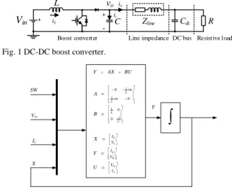
Fig. 1 shows a DC-DC boost converter with ideal components and constant input voltage connected to a DC bus through a line impedance. Using HSS model [1][2], the boost converter can be described as 1 1 1 1 0 0 SW SW in L L L L o o C C N V sI I sVo N V − I − − = + − (1) where IL = [IL-k … IL-1, IL0 , IL1, … ILk]T, N = diag[-jkω0 … -jω0,
0 , jω0, … jkω0] and Vo, Vin, Io has the same form of IL. From (1),
the HSS model of DC-DC boost converter can be derived and the corresponding HSS model block diagram is depicted in Fig. 2.
3. HSS Model of Output Impedance
In this section, an attempt to obtain the HSS model of output impedance for DC-DC boost converter is described. First, small-signal perturbations is included in the circuit diagram which is redrawn as in Fig. 3. Next, block diagram of the system in Fig. 3 is drawn in Fig. 4 with considering HTF matrices of converter and controller [3].
The output impedance is defined as o
Z
=v
o /i
o (2)where
v
o andi
o are small-signal output voltage and current perturbations, respectively. Based on block diagram in Fig. 3 and assuming the constant input voltage vin, the output impedance witha current control can be expressed as
(
)
1PWM d
o H H Gv i G I op
Z = + − Z (3)
where I is an identity matrix and Hv, Hi, GPWM, Gd, and Zop are
HTF matrices of voltage control, current control, PWM comparator, duty-to-output and open-loop output impedance, respectively. The HTF matrix of Zo has the matrix form of
0 1 2 1 1 2 1 0 ( ) ( ) ( ) ( ) ( ) ( ) ( ) ( ) ( ) ( ) o s o o s o o s o o s o s o o s Z s j Z s Z s j Z s Z s j Z s Z s j Z s j Z s Z s j − − − + − + = − + − + (4) L C Vin iL R ic io + + -Zline vo Cdc
DC bus Resist ive l oad Line impedance
Boost convert er Fig. 1 DC-DC boost converter.
SW Vin Io Y
1 1 1 1 0 0 SW SW L C L C L o L in o N N I V I Vo V I Y AX BU A B X Y U − = + − − − = = = = = X
Fig. 2 HSS model of DC-DC boost converter.
L C Vin R iL ic io + vin(t) ~ io(t) ~ + -v~o(t) Zline vo
Fig. 3 Circuit diagram for modelling of output impedance.
GSW + + vin GPWM vc d Gvd iL Hi + ZOP vo io + -Hv + -Gid ~ ~ ~ ~ ~ ~
Fig. 4 Block diagram for modelling of output impedance.
455
4. Simulation Results and Stability Analysis
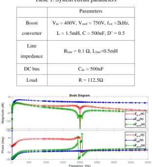
Simulations have been performed in Matlab/Simulink and Plexim/PLECS software to verify the stability analysis of DC-DC boost converter based on HSS model of output impedance. Table 1 lists the parameters in.
Fig. 5 shows the Bode plot of output impedance using HSS model plotted in Matlab. The plot contains three curves, each represents Zo-1(s), Zo0(s), and Zo+1(s) respectively, all of them are
matrix elements of output impedance Zo. It can be seen in the plot
that there are frequencies of Zo0 less than 500 Hz and also
frequencies of Zo-1 and Zo+1 around the switching frequency
crossing 90o in which passivity stability criteria is violated and
therefore can make the output voltage unstable. Perturbation frequencies in the range of 500 Hz – 1500 Hz are considered stable.
Fig. 6 shows output voltage and current waveforms performed in PLECS using switching model when the output current is perturbed with perturbation frequency 120 Hz and 1000 Hz. It can be seen that in the first perturbation of current (120Hz < 500 Hz), distortions appear at the output voltage (unstable), whereas in the second perturbation (1000Hz), distortions do not (stable). This result corresponds well with the Bode plot of output impedance.
Fig. 7 output voltage and current waveforms in HSS model using Simulink when the same parameters and conditions are applied to the simulation. Fig. 7(a) shows the DC component of output voltage (vo0) and output current (io0), whereas Fig. 7(b)
shows the harmonic components. It can be seen during the first perturbation, distortions appear both at the output voltage and current while during the second perturbation, the output voltage is not distorted. The waveforms in Fig. 7 match with those of in Fig. 6 and with the Bode plot of output impedance in Fig. 5.
5. Conclusions
This paper has modeled the output impedance of boost converter using HSS model. Bode plot of output impedance has been drawn in Matlab. Simulation results verified the output voltage and current waveforms under perturbations match well with the output impedance derived using HSS model.
This research was supported by Korea Electric Power Corporation. (Grant number : R18XA06-35).
References
[1] J.-B. Kwon, X. F. Wang, F. Blaabjerg and C. L. Bak, “Frequency domain modeling and simulation of DC power electronic systems using harmonic state space method,”
IEEE Trans. Power Electron., vol. 32, pp. 1044-1055, 2017.
[2] M. Kamalirad, D. D. To and D.-C. Lee, “Harmonic State Space Modeling of DC Microgrid Systems,”전력전자학술 대회논문집, 2019.
[3] X. Yue, X. Wang and F. Blaabjerg, “Review of Small-Signal Modeling Methods Including Frequency-Coupling Dynamics of Power Converters,” IEEE Trans. Power
Electron., vol. 34, no: 4, pp. 3313-3328, 2019.
[4] X. Wang 그리고 F. Blaabjerg, “Harmonic Stability in Power Electronic-Based Power Systems: Concept, Modeling, and Analysis,” IEEE Trans. Smart Grid, vol. 10, no: 3, pp. 2858-2870, 2019.
Table 1. System circuit parameters
Parameters Boost converter Vin = 400V, Voref = 750V, fsw =2kHz, L = 1.5mH, C = 500uF, D’ = 0.5 Line impedance Rline = 0.1 Ω, Lline=0.5mH DC bus Cdc = 500uF Load R = 112.5Ω
Fig. 5 Bode plot of output impedance.
120 Hz perturbation 1000 Hz perturbation
Fig. 6 Output voltage and current waveforms (switching model).
(a) DC component
120 Hz perturbation 1000 Hz perturbation
(b) Harmonics components Fig. 7 Output voltage and current waveforms (HSS model).