63-2 / S. Reineke
• IMID 2009 DIGEST
Abstract
Recently,electroluminescence devices based on organic semiconductors have made considerable progress. Displays based on organic light emitting diodes (OLED) are commercially available. To gain broader acceptance, the performance of OLED devices has to be further improved, in particular for lighting. This article discusses the possibility to use controlled electrical doping for improving the properties of devices and new approaches for highly efficient white OLED.
1. Introduction
Organic semiconductors are a novel materials class which is characterized by a large variety of possible materials and the ability to be deposited on low-cost and flexible substrates. Organic semiconductors are currently investigated intensively, both because the basic physics are little understood and because of attractive application possibilities, such as flat-panel displays based on organic light emitting diodes (OLED).
Despite the fact that organic semiconductors have, in particular as thin films, rather low mobilities, they perform surprisingly well in optoelectronic devices. Surprisingly, doping (for raising the conductivity) has been largely ignored till now in organic devices, in contrast to classical semiconductor technology where controlled n- and p-type doping has always been a standard technique needed for virtually all devices, in particular for efficient LED.
In the past few years, we have intensively worked on doping of organic semiconductors and have shown that stable and reproducible doping can be achieved. The performance of devices can be considerably improved by including electrically doped layers.
Recently, we have been able to demonstrate white OLED with extremely high efficiency using this concept.
2. Basics of Doping
Here, we briefly discuss some key results from our work in Dresden on the basic physics of and devices with doped transport layers. For a detailed discussion, we refer to the review by Walzer et al. /1/.
The doping of organic semiconductors is actually known since a long time, using gases or small molecules (see, e.g. /2/). An alternative approach is using e.g. alkali metals /3/. However, this approach has the disadvantage that it tends to unstable at higher temperature, also, there are difficulties with manufacturing.
In our work, we have used larger organic molecules to avoid diffusion effects. The basic step in realizing molecular electrical doping is to achieve a charge transfer from the organic semiconductor molecule to the dopant (p-doping, /4/) or from the dopant molecule to the matrix (n-doping /5,6/). In the first case, the lowest unoccupied orbital (LUMO) of the dopant must be below the highest occupied orbital of the semiconductor matrix, in the second case the other way round. Especially for materials with high-lying LUMO, like electron transporters for OLED, the synthesis is difficult and only proprietary materials /7/ are yet available.
As shown in /4/, it is possible to raise the conductivity by orders of magnitude in a very controlled manner. This leads to lower ohmic losses. Another aspect is that the contact resistance at electrodes can be drastically reduced since the thin space charge barriers can be tunneled through easily by the charges /8/. This is particular interesting for
New approaches towards highly efficient OLED
S. Reineke, R. Meerheim, Q. Huang, G. Schwartz, B. Lüssem, K. Leo
1
Institut für Angewandte Photophysik, Technische Universität Dresden, 01062 Dresden, Germany
Tel.:49-351-46334389, E-mail: leo@iapp.de
63-2 / S. Reineke
IMID 2009 DIGEST • OLED on other substrates than ITO, where the control
of the work function is difficult.
3. Applications in OLED
As argued above, these electrical doping concepts can be successfully applied in devices: the concept of molecular doping allowed to realize green OLED devices with the highest efficiencies reported so far /9/, well exceeding the efficiency of current inorganic GaN devices! The devices were pin-devices where the emitting layer is embedded between a p-doped hole transport layer and an n-doped electron transport layer. It has been shown that these pin-structures can also achieve extremely long lifetimes /10/, i.e. there is no negative effect on the device lifetime by dopand diffusion or other effects.
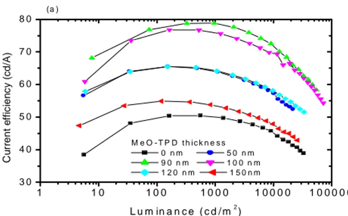
Doped transport layers are particularly useful for devices which are top-emitting, i.e. emit away from the substrate. Here, it is important to optimize the microcavity which is formed by the usually reflecting back contact and the semi-transparent top contact. We have recently shown that using doped layers, very efficient top emitting OLED can be realized /11,12/. Figure 1 shows that by using an additional transparent organic outcoupling layer (MeO-TPD in this case), the efficiency can be further improved.
Another are where the doping concepts are very useful is the realization of stacked OLED, where the interconnection contacts can be efficiently realized with molecularly doped layers.
Fig. 1: Current efficiency of a top-emitting green OLED as a function of Luminance and outcoupling layer thickness.
4. White OLED:
How to beat the fluorescent tube
White OLED have recently achieved very high efficiencies /13,14/, opening the path to a new form of high-efficiency area lighting devices. Surprisingly, the field of OLED is currently dominated by evaporated small-molecule devices, despite the fact that initially, polymer OLED which allow liquid processing were seen as the more direct and cost-effective approach to devices. One of the reasons is that the doping techniques described here a much easier to apply in vacuum processing.
To obtain white OLED with very high efficiency, we have recently employed a triplet harvesting concept which yields quantum efficiency of up to unity despite using fluorescent emitters /15/. By using an energetically high-lying triplet transition of the blue emitter which also acts as host, this concept avoids losses due to triplet transfer to a blue emitter /13/. This concept has the particular advantage that no phosphorescent blue emitter is needed, being still a challenge in materials development.
Furthermore, we here discuss some new results on all phosphorescent white OLED /14/ with efficiency of 90lm/W for a flat device at 1000 Cd/m2, clearly beating fluorescent tubes in efficiency for the first time. For the realization of such devices, the availability of stable blue phosphorescent emitter is however still a challenge.
The key approaches for this efficiency were
• optimizing the emission zone, using suitably chosen materials and specially designed interlayers and
• using a high-index substrate with a suitable flat high-index outcoupling structure.
The optimized emission zone (see Figure 2) with spatially distributed exciton recombination zone also leads to very low roll-off at high intensity: Our device still achieves 74lm/W even at 5000 Cd/m2. This demonstrates that OLED lighting can also be used for high brightnesses, which reduces cost because less area is needed.
1 1 0 1 0 0 1 0 0 0 1 0 0 0 0 1 0 0 0 0 0 3 0 4 0 5 0 6 0 7 0 8 0 (a ) C u rr ent e ff ic ien c y ( c d/ A) L u m in a n c e ( c d / m2) M e O - T P D t h i c k n e s s 0 n m 5 0 n m 9 0 n m 1 0 0 n m 1 2 0 n m 1 5 0 n m
63-2 / S. Reineke
• IMID 2009 DIGEST
Fig. 2: Layer design of the white OLED structure /14/.
The high index substrate reduces thin-film modes since the refractive index step to the substrate is reduced. However, to fully exploit this advantage, it is also necessary to use a thick electron transport layer (approximately 200nm) to reduce the coupling to plasmonic modes on the cathode. To still keep the good electrical properties of the devices, a doped layer is needed /14/.
Figure 3 shows the power efficiencies of a device with low-index (LI) substrate and a device with high-index (HI) substrate. It is clearly visible that the HI device is superior. For the flat device with outcoupling, the 90lm/W are reached, for a device with a glass sphere more than 150lm/W at low brightness are reached, showing that there is still room for further improvement if the outcoupling from the substrate using flat outcoupling structures can be improved and if the roll-off is further reduced. Also, the color coordinates of the devices need to be improved: With the sky-blue emitter employed here, the devices emit a yellowish white. For coordinates on the Planckian curve, deep blue phosphorescent emitters which are not yet available are needed.
5. Conclusions
Using suitable dopant molecules, it is possible to dope organic semiconductors in a manner very similar to their inorganic counterparts. The technique of controlled doping of organic semiconductors has led to clear improvements in the performance of devices, in particular OLED. Highly efficient white OLED using doped transport layers exceed the efficiency of fluorescent tubes. It is to be expected that in the future,
other novel devices will be designed which use this technique.
.
4. Summary
Fig. 3: Power efficiency of the low-index (top) and high-index substrate device (bottom). For the LI device, the lower line is without any outcoupling and the upper line for a half sphere, for the HI device, the lowest line is without outcoupling, the middle line with a flat outcoupling structure, and the uppermost line for a halfsphere /14/.
Acknowledgement
The authors would like to thank the many coworkers who have made possible these studies. Among the many people, I would in particular like to thank Martin Pfeiffer, Jan Blochwitz-Nimoth, Jens Drechsel, Torsten Fritz, Kentaro Harada, Gufeng He, Fenghong Li, Ansgar Werner, Xiang Zhou, and many others which cannot be mentioned here. Finally, we acknowledge the funding by the EC, German Ministry for Education and Research, German Ministry for
63-2 / S. Reineke
IMID 2009 DIGEST • Economy and Labor, State of Saxony, and the
Deutsche Forschungsgemeinschaft for the support via the Leibniz Prize.
6. References
1. K. Walzer, B. Maennig, M. Pfeiffer M, K. Leo, Chem. Rev. 107, 1233 (2009)
2. Y. Yamamoto; K. Yoshino, Y. Inuishi, J. Phys. Soc. of Jap. 47, 1887 (1979).
3. J. Kido, T. Matsumoto, Appl. Phys. Lett. 73, 2866 (1998)
4. M. Pfeiffer, A. Beyer, T. Fritz, K. Leo K. Appl. Phys. Lett. 73, 3202 (1998).
5. Nollau, M. Pfeiffer, T. Fritz, K. Leo, J. Appl. Phys. 87, 4340 (2000).
6. A.G. Werner, F. Li, K. Harada, M. Pfeiffer, T. Fritz, K. Leo, Appl. Phys. Lett. 82, 4495 (2003).
7. Novaled AG, www.novaled.com
8. J. Blochwitz, M. Pfeiffer, T. Fritz, K. Leo, D.M. Alloway, P.A. Lee, N.R. Armstrong, Org. Electronics 2, 97 (2001).
9. G. He, M. Pfeiffer, K. Leo, M. Hofmann, J. Birnstock, R. Pudzich, J. Salbeck, Appl. Phys. Lett. 85, 3911 (2004).
10. R. Meerheim, K. Walzer, M. Pfeiffer, K. Leo, Appl. Phys. Lett. 89, 061111 (2006).
11. Q. Huang, S. Reineke, K. Walzer, M. Pfeiffer, and K. Leo, Appl. Phys. Lett. 89, 263512 (2006).
12. Q. Huang, K. Walzer, M. Pfeiffer, V. Lyssenko, G. He, and K. Leo, Appl. Phys. Lett. 89, 113515 (2006).
13. Y. Sun, N.C. Giebink, H. Kanno, B. Ma, M.E. Thompson, S.R. Forrest, Nature 440, 908 (2006)
14. T. Nakayama, K. Hiyama, K. Furukawa, H.Ohtani, Society for Information Display 2007 International Symposium (Digest of technical papers Vol.38, p.1018).
15. G. Schwartz, M. Pfeiffer, S. Reineke, K. Walzer, K. Leo, Adv. Mat. 19, 3672 (2007) 16. S. Reineke, F. Lindner, G. Schwartz, N.
Seidler, K. Walzer, B. Lüssem, Nature 459, 234 (2009).