with Ultra-Thin Passivation Layer
for High-Performance Transistors
Based on Two-Dimensional
Semiconductor Channels
Hyunjin Jo
1, Jeong-Hun Choi
1, Cheol-Min Hyun
1, Seung-Young Seo
2, Da Young Kim
3,
Chang-Min Kim
3, Myoung-Jae Lee
4, Jung-Dae Kwon
5, Hyoung-Seok Moon
6, Se-Hun Kwon
3&
Ji-Hoon Ahn
1We propose a hybrid gate structure for ion gel dielectrics using an ultra-thin Al2O3 passivation layer for
realizing high-performance devices based on electric-double-layer capacitors. Electric-double-layer transistors can be applied to practical devices with flexibility and transparency as well as research on the fundamental physical properties of channel materials; however, they suffer from inherent unwanted leakage currents between electrodes, especially for channel materials with low off-currents. Therefore, the Al2O3 passivation layer was introduced between the metal electrodes and ion gel film as a leakage
current barrier; this simple approach effectively reduced the leakage current without capacitance degradation. In addition, we confirmed that a monolayer MoS2 transistor fabricated with the proposed
hybrid gate dielectric exhibited remarkably enhanced device properties compared to a transistor using a normal ion gel gate dielectric. Our findings on a simple method to improve the leakage current properties of ion gels could be applied extensively to realize high-performance electric-double-layer transistors utilizing various channel materials.
Ionic liquids provide the advantage of very large capacitances by the formation of nanogap capacitors at solid– liquid interfaces1,2, and electric double-layer-transistors (EDLTs) using ionic liquids have received significant
attention because they show ultra-high capacitance and potential applicability in both practical flexible and transparent devices and studies on the fundamental physical properties of channel materials, including carrier transport phenomena, superconductivity, and thermoelectricity3–13. Despite this broad applicability, ionic liquids
are limited in application to practical devices because of fluidity-related instability; however, this problem can be solved by introducing an ion gel, comprising a mixture of an ionic liquid and a polymer network, which maintains both the mechanical flexibility of the polymer and the large specific capacitance of the ionic liquid14–19. As
demon-strated by printable and photo-patternable ion gels, large-area device integration and the realization of practical applications of stretchable and flexible devices have become possible20,21.
1Department of Electronic Material Engineering, Korea Maritime and Ocean University, 727 Taejong-ro, Yeongdo-gu, Busan, 49112, Republic of Korea. 2Department of Material Science and Engineering, Pohang University of Science and Technology, 77 Cheongam-Ro, Pohang, 790-784, Republic of Korea. 3School of Materials Science and Engineering, Pusan National University, 30 Jangjeon-Dong Geumjeong-Gu, Busan, 609-735, Republic of Korea. 4Daegu Gyeongbuk Institute of Science and Technology (DGIST), 333 Techno Jungang Daero, Hyeonpung-Myeon, Dalseong-Gun, Daegu, 42988, Republic of Korea. 5Department of Advanced Functional Thin Films, Surface Technology Division, Korea Institute of Materials Science, 797 Changwondaero, Sungsan-Gu, Changwon, Gyeongnam, 51508, Republic of Korea. 6Energy Plant R&D Group, Korea Institute of Industrial Technology (KITECH), 30 Gwahaksandan 1-ro 60beon-gil, Gangseo-gu, Busan, 46742, Republic of Korea. Hyunjin Jo, Jeong-Hun Choi and Cheol-Min Hyun contributed equally to this work. Correspondence and requests for materials should be addressed to S.-H.K. (email: [email protected]) or J.-H.A. (email: [email protected])
Received: 23 August 2017 Accepted: 9 October 2017 Published: xx xx xxxx
Meanwhile, in recent years, thin-film transistors (TFT) based on two-dimensional (2D) materials, such as hexagonal metal dichalcogenides, have been extensively studied for their potential applicability in emerg-ing electronic and optoelectronic devices22–25. 2D material-based TFTs using ion gels as gate dielectrics have
been reported to exhibit superior electrical properties, such as low threshold voltages, high carrier mobilities, transparency, and flexibility26–29. Braga et al. realized ambipolar transistors fabricated using exfoliated WS
2
flakes with ionic liquid and proposed a method to determine the bandgap size directly30; Zhang et al.
demon-strated the formation and detection of field-induced p-n junctions in MoS2 EDLTs31. Thus, ion gels as gate
die-lectrics for 2D material-based devices have several advantages, but their practicality must be improved to realize high-performance devices. Electric double-layer dielectrics, including ion gels, exhibit high leakage current levels between the gate and source/drain electrodes compared to those in inorganic-based gate dielectric32. For channel
materials with greater gate leakage currents than intrinsic off-current levels leakage not only degrades the on/ off characteristics of the devices but also increases the threshold voltage. For example, the off-current level of previously reported monolayer MoS2 transistors was in the range of 10−10–10−12 A33–36, which is less than the
gate leakage current level of several nano-amperes at the operating voltage in ion-gel-gated devices32,37. Most
reported ion-gel-gated transistors with 2D materials exhibit off-current levels exceeding the nano-ampere range, which might be greater than the intrinsic properties of the channel materials; in such cases, the transfer curves are expressed on linear rather than logarithmic scales. Therefore, it is important to reduce the leakage current through ion-gel dielectrics between the gate and source/drain electrodes to achieve higher-performance devices, particularly for channel materials with low off-current levels.
In this study, we propose a hybrid gate dielectric structure composed of an ion-gel film and ultra-thin Al2O3 passivation layer deposited by atomic layer deposition (ALD) to improve the electrical properties of the
ion-gel-based 2D transistor, because Al2O3 films exhibit good leakage current properties and the ultra-thin Al2O3
layer can act as a leakage current barrier without causing significant capacitance drops38–40. Moreover, it is known
that the ultra-thin Al2O3 films formed by ALD exhibit flexibility and transparency35,41, and therefore the hybrid
dielectric structure could be suitable for application to flexible and transparent devices. To optimize the structure of the hybrid dielectrics, the variations in the electrical properties of the Al2O3 layer-modified ion gel film were
systemically investigated as a function of the thickness of the Al2O3 passivation layer. Finally, the optimized
die-lectric structure was applied to a monolayer MoS2 transistor and compared to a transistor using a normal ion-gel
gate dielectric to confirm the effect of the proposed hybrid dielectrics on the transistor performance.
Results and Discussion
The ion gel films were prepared from a solution of the triblock copolymer poly(styrene-block-methyl methacrylate-block-styrene) (PS-PMMA-PS) and the ionic liquid 1-ethyl-3-methylimi dazolium bis(trifluo-romethylsulfonyl)imide ([EMIM][TFSI]), in ethyl propionate as an organic solvent. The PS-PMMA-PS and [EMIM][TFSI], with molecular structures as shown in Fig. 1a, are commonly used base materials to fabricate ion gels for EDLTs28,29. First, we fabricated simple two-terminal devices, as shown in Fig. 1b,c, to investigate the effect
of Al2O3 passivation on the electrical properties of the ion-gel films. The ultra-thin Al2O3 layers were deposited by
thermal ALD using H2O as an oxidant at the temperature of 350 °C. The reasons for determining the deposition
conditions of ALD-Al2O3 will be discussed later. Figure 1d shows the current (I)–voltage (V) characteristics of the
two-terminal devices according to the thicknesses of the inserted Al2O3 layers between the metal electrodes and
ion gels. With the insertion of the Al2O3 passivation layer, the leakage current is remarkably decreased. When the
dielectric film comprises only the ion gel without a passivation layer, the current level at 1 V is ~10−9 A, indicating
difficulty in accurately measuring the on/off characteristics for EDLTs devices with off-current levels below the nano-ampere scale. As shown in Fig. 1e and the inset of Fig. 1d, the current levels through the hybrid dielectric films exponentially decrease as the Al2O3 thickness is increased to 10 nm. This confirms that the leakage current
can be effectively reduced by more than two and three orders of magnitude by inserting Al2O3 layers of only 3 and
5 nm in thickness, respectively.
Figure 1. (a) Molecular structures of the triblock copolymer (PS-PMMA-PS) and ionic liquid ([EMIM]
[TFSI]) used for preparation of ion-gel film. (b) Schematic and (c) optical micrograph of the two-terminal device for characterization of electrical properties of hybrid dielectrics. (d) Current–voltage characteristics of hybrid dielectrics with various Al2O3 layer thicknesses. Inset: log-scale plot. (e) The variation of current density
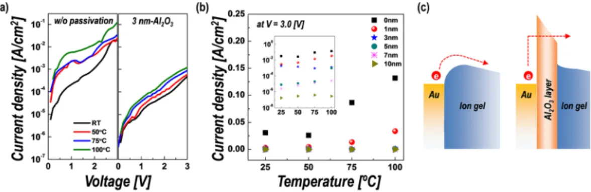
Furthermore, we investigated the temperature dependence of the leakage current through the hybrid ion-gel films to study the change of current mechanism caused by the insertion of the Al2O3 layer. Figure 2a shows the
current density (J)–voltage (V) characteristics of the ion gel-based dielectric films without and with a 3-nm-thick Al2O3 passivation layer measured at the temperature range of room temperature to 100 °C. With the insertion of
the ultra-thin Al2O3 layer, not only the overall leakage current level decreases, but also the temperature
depend-ency of the current is decreased (data for samples with different passivation thicknesses is shown in Fig. S2 of the Supplementary Information). As indicated in Fig. 2b, the temperature dependency of the leakage current tends to decrease with increasing thickness of the Al2O3 passivation layer. Based on these observations, the current
mechanism and the cause of the decrease in the leakage current by Al2O3 passivation can be explained as follows:
In the absence of a passivation layer, the leakage current flows mainly by a thermionic mechanism, in which elec-trons flow over a specific barrier height between the metal electrode and the ion-gel dielectrics. However, the thin but large-bandgap (~8.9 eV) Al2O3 passivation layer located between the metal electrode and the ion gel acts as a
leakage current barrier, preventing the flow of a direct thermionic current. Therefore, as the thickness of the pas-sivation layer increases, the main current mechanism through the metal electrode to the ion gel-based dielectrics changes to electric field-induced tunneling, which is relatively insensitive to temperature, as indicated in the sche-matics in Fig. 2c. The results confirm that the leakage current characteristics are effectively improved by reducing the thermionic current in the dielectric structure with the placement of a large-bandgap Al2O3 passivation layer.
Meanwhile, although the leakage current characteristics of the device using a hybrid dielectric structure of ion gel with an Al2O3 passivation layer can be improved, the dielectric constant of Al2O3 is relatively low (~9),
which can degrade the dielectric properties of the device. Therefore, we investigated the dielectric properties of ion gel-based hybrid dielectrics as a function of the thickness of the inserted Al2O3 layer. The capacitance density
of the ion gel without passivation layer was ~10.8 μF/cm−2, which is comparable to those of previously reported
gels (~5–10 μF/cm−2)4,29,37. The capacitance slightly increased by the insertion of an Al
2O3 layer with the thickness
of ~3 nm and then continuously decreased with further increases in the inserted Al2O3 thickness. The decrease in
capacitance for relatively thick (>5 nm) Al2O3 layers can be explained by the relatively small dielectric constant
of Al2O3 films, but it is difficult to understand the increase in capacitance for 3-nm-thick Al2O3-inserted ion-gel
films. However, it was previously reported that self-discharge at the charged state in electric double-layer capaci-tors, caused by high leakage currents, could cause capacitance drops42,43. Therefore, the increase in capacitance for
the sample with the 3-nm-thick Al2O3 layer was attributed to the decrease in leakage current by the insertion of
the leakage current barrier. It is also observed that the frequency dependence of the capacitance tends to decrease with increases in the thickness of the Al2O3 passivation layer (see inset of Fig. 3). The most important point is
that, although the low-dielectric-constant layer is inserted, the capacitance is not degraded until the Al2O3
thick-ness is increased to ~5 nm. Therefore, it can be expected that the hybrid gate structure of ion-gel dielectrics with ultra-thin Al2O3 passivation layers could effectively improve the transistor characteristics of EDLTs by reducing
the gate leakage current without inducing capacitance drops.
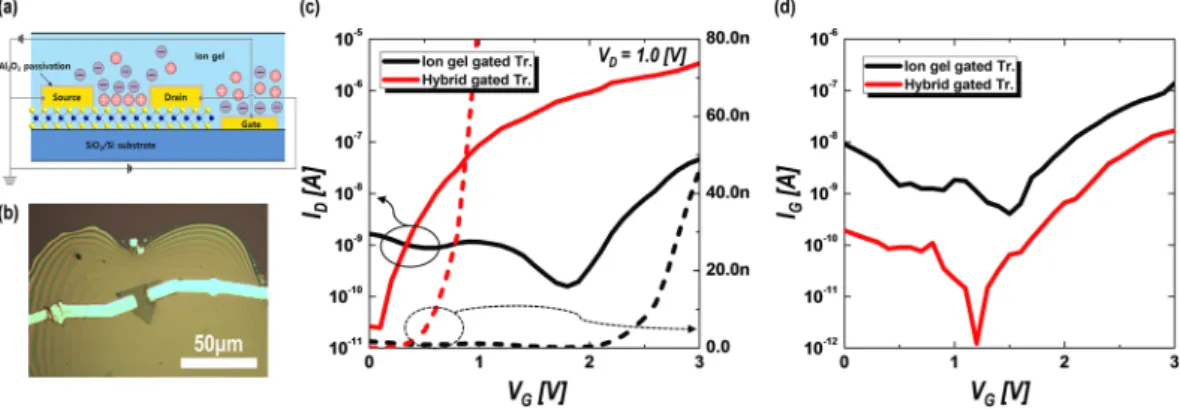
Finally, the hybrid gate dielectric of ion-gel film with an ultra-thin Al2O3 passivation layer was applied to
MoS2 EDLTs to confirm the effect of the proposed gate structure on the performance of the MoS2 transistors.
Figure 4a,b show the schematic and optical micrograph of the fabricated MoS2 EDLT structure using the hybrid
gate dielectric, respectively. Monolayer MoS2 crystals directly grown on a SiO2/Si substrate by chemical vapor
deposition (CVD) were used as a transistor channel; source/drain and side gate electrodes were defined by the lift-off method. After formation of electrodes, 3-nm-thick Al2O3 layers were deposited by thermal ALD at 350 °C.
ALD Al2O3 films are usually obtained using H2O, O3, or O2 plasma as the oxidant at the temperature range of 50
to 400 °C. In our case, we used H2O vapor as an oxidant to prevent damage to the MoS2 channel by ozone or O2
plasma. In addition, because ideal van der Waals 2D materials do not have dangling surface bonds, the precursor molecules for ALD growth were infrequently adsorbed on the 2D materials, so that thin film growth by ALD could be suppressed on the 2D materials. Therefore, the ALD-Al2O3 layer could be selectively deposited except
on the 2D material surface without additional etching processes. However, the CVD-grown MoS2 could contain
defect sites where the precursor can chemosorb; therefore, the ALD process for depositing the Al2O3 passivation
layer was conducted at the temperature of 350 °C to minimize the chemisorption of precursors on the MoS2
Figure 2. (a) J–V characteristics of ion gel film without passivation and with 3-nm-thick Al2O3 passivation
layer, measured from room temperature to 100 °C. (b) Temperature-dependent current density of hybrid structure with various thicknesses of Al2O3 passivation layer, measured at 3 V bias. Inset: log-scale plot. (c)
surface44. After the deposition of the 3-nm-thick Al
2O3 layer by ALD on the MoS2 crystals, it was confirmed that
the Al2O3 layer was rarely deposited on the surface of the MoS2 crystals by atomic force microscopy analysis (see
Fig. S3 of the Supplementary Information). In fact, since no degradation of capacitance was observed for inserted Al2O3 layer thicknesses below ~5 nm, it can be expected that even if the ultra-thin Al2O3 is partially deposited on
MoS2, the transistor performance would not be negatively affected. The room-temperature transfer characteristics
(ID–VG) of the MoS2 EDLTs measured at the source–drain voltage (VD) of 1.0 V with and without Al2O3
passi-vation are indicated in Fig. 4c. For comparison, regardless of with and without passivation, the channel length and width were fixed at 10 and 10 μm, respectively. Whereas the on/off ratio of the ion gel-only gated transistor is ~102 because of the relatively high off-current level of ~10−9 A, the on/off ratio of the hybrid-gated transistor is
remarkably increased to ~105. Moreover, it is observed that the threshold voltage is decreased by more than 2 V,
and the subthreshold swing (SS) is also improved by inserting the ultra-thin Al2O3 layer between the electrodes.
These improvements in the electrical properties of the transistor by the Al2O3 passivation layer are mainly
attrib-uted to the reduction of the leakage current between the gate and source/drain electrodes. By applying the hybrid gate structure of ion-gel dielectrics with 3-nm-thick Al2O3 passivation layers, as shown in Fig. 4d, the gate leakage
current is significantly decreased by about two orders of magnitude (from several nano-amperes to several tens of pico-amperes at ID = 1.0 V), which well corresponds with the off-current level of each transistor. In addition,
the on-current level of the hybrid gated EDLTs was also greatly increased by Al2O3 passivation, which might be
attributed to the reduced dielectric loss from the reduced gate leakage current.
Conclusions
In this study, we systematically investigated the effect of inserting an Al2O3 passivation layer between the ion-gel
dielectric film and metal electrode on the electrical properties of a transistor to propose a hybrid ion gel-based gate structure with improved properties. As the thickness of the inserted Al2O3 layer was increased, the leakage
current through the ion gel-based dielectrics was exponentially decreased (more than two orders of magnitude even with an ultra-thin Al2O3 layer of 3 nm in thickness). Moreover, no degradation of capacitance was observed for
Figure 3. The variation of the capacitance density of two-terminal device with hybrid dielectrics depending
on Al2O3 layer thickness with frequency of 10 kHz. Inset: frequency dependence of the capacitance for different
Al2O3 thickness.
Figure 4. (a) Schematic and (b) optical micrograph of the hybrid-structure EDLTs fabricated using monolayer
single-crystalline MoS2. (c) Transfer curve and (d) gate leakage current (absolute values) of the MoS2 EDLTs
without passivation (ion gel gated Tr.) and with 3-nm-thick Al2O3 passivation layer (Hybrid gated Tr.) measured
at drain voltage of 1.0 V under room temperature. Solid line and dashed line in transfer graph indicate the logarithmic-scale (left-side axis) and linear-scale (right-side axis) value of drain current, respectively.
and then the mixture was sonicated to obtain a homogeneous solution. This solution was drop-casted onto the metal electrodes of the device. Through annealing at 120 °C for 10 min, the solvent was evaporated and an ion gel film was formed through the physical association of the polymer blocks in the ionic liquid.
Deposition of ultra-thin Al
2O
3layer.
To enhance the electrical properties of the gate dielectric based onthe ion gel, an ultra-thin Al2O3 layer, deposited by ALD at 350 °C, was introduced between the metal electrode
and ion-gel interface. Trimethylaluminum (TMA, Al(CH3)3) and water vapor (H2O) were used as precursor and
oxidant, respectively; both canisters containing TMA and H2O were maintained at the temperature of 10 °C. The
deposition process was performed under saturation conditions. One deposition cycle consisted of the exposure of TMA for 0.5 s, purging with N2 for 5 s, exposure of H2O for 0.5 s, and purging with N2 for 5 s.
Device fabrication and characterization.
To investigate the effect of Al2O3 passivation on the electricalproperties, a simple two-terminal device was fabricated on SiO2/Si substrate. First, two electrodes were formed
from 10-nm Ti/50-nm Au layers via a lift-off method using photolithography (Photo resist: AZ5214, AZ Electronic Materials) and e-beam evaporation. The hybrid gate dielectric was formed via the deposition of ultra-thin Al2O3
layers with thicknesses of 0–10 nm, followed by the drop-casting of the ion gel. Meanwhile, to apply the hybrid gate dielectric to field-effect transistor (FET) devices, MoS2 transistors were fabricated using monolayer crystals
syn-thesized by CVD (see Fig. S1 of the Supplementary Information for more details on the synthesis process). Similar to the above method, source/drain and side gate electrodes were formed from 10-nm Ti/50-nm Au layers by a lift-off method. In this case, however, electron-beam lithography using poly(methyl methacrylate) (PMMA) was used instead of photolithography, because the source/drain electrodes required greater accuracy in formation on the MoS2 crystal. Finally, for comparison, two types of ion gel-based gate dielectrics were formed, one without
pas-sivation and the other with a 3-nm-thick Al2O3 passivation layer. After the device fabrication, capacitance–voltage
(C–V), current–voltage (I–V), and FET transfer characteristics measurements were performed in a dark probe sta-tion using a semiconductor characterizasta-tion system (Keithley, 4200-SCS).
References
1. Yuan, H. et al. Electrostatic and Electochemical Nature of Liquid-Gated Electric-Double-Layer Transistor Based on Oxide Semiconductor. J. Am. Chem. Soc. 132, 18402–18407 (2010).
2. Du., H., Lin, X., Xu, Z. & Chu, D. Electric Double-Layer Transistors: A Review of Recent Progress. J. Mater. Sci. 50, 5641–5673 (2015).
3. Perera, M. M. et al. Improved Carrier Mobility in Few-Layer MoS2 Field-Effect Transistors with Ionic-Liquid Gating. ACS Nano 7, 4449–4458 (2013).
4. Ye, J. T. et al. Liquid-Gated Interface Superconductivity on an Atomically Flat Film. Nat. Mater. 9, 125–128 (2010).
5. Yuan, H. et al. High-Density Carrier Accumulation in ZnO Field-Effect Transistor Gated by Electric Double Layer of Ionic Liquid.
Adv. Funct. Mater. 19, 1046–1053 (2009).
6. Fujimoto, T. & Awaga, K. Electric-Double-Layer Field-Effect Transistor with Ionic Liquids. Phys. Chem. Chem. Phys. 15, 8983–9006 (2013).
7. Zhang, Y., Ye, J., Matsuhashi, Y. & Iwasa, Y. Ambipolar MoS2 Thin Flake Transistor. Nano Lett. 12, 1136–1140 (2012). 8. Allain, A. & Kis, A. Electron and Hole Mobility in Single-Layer WSe2. ACS Nano 8, 7180–7185 (2014).
9. Xia, Y., Cho, J. H., Lee, J., Ruden, P. P. & Frisbie, C. D. Comparison of the Mobility-Carrier Density Relation in Polymer and Single-Crystal Organic Transistors Employing Vacuum and Liquid Gate Dielectrics. Adv. Mater. 21, 2174–2179 (2009).
10. Yanagi, K. et al. Tuning of the Thermoelectric Properties of One-Dimensional Material Networks by Electron Double Layer Techniques Using Ionic Liquids. Nano Lett. 14, 6437–6442 (2014).
11. Choi, J.-H., Xie, W., Gu, Y., Frisbie, C. D. & Lodge, T. P. Single Ion Conducting, Polymerized Ionic Liquid Triblock Copolymer Films: High Capacitance Electrolyte Gates for n-type Transistors. ACS Appl. Mater. Interface 7, 7294–7302 (2015).
12. Yuan, H. T. et al. Liquid-Gated Electric-Double-Layer Transistor on Layered Metal Dichalcogenide, SnS2. Appl. Phys. Lett. 98, 012102 (2011).
13. Lei, B. et al. Evolution of High-Temperature Superconductivity from a Low-Tc Phase Tuned by Carrier Concentration in FeSe Thin Flakes. Phys. Rev. Lett. 116, 077002 (2016).
14. Lee, J., Panzer, M. J., He, Y., Lodge, T. P. & Frisbie, C. D. Ion Gel Gated Polymer Thin-Film Transistors. J. Am. Chem. Soc. 129, 4532–4533 (2007).
15. Lee, J. et al. Ion Gel-Gated Polymer Thin-Film Transistors: Operating Mechanism and Characterization of Gate Dielectric Capacitance, Switching Speed, and Stability. J. Phys. Chem. C. 113, 8972–8981 (2009).
16. Xu, F. et al. Highly Stretchable Carbon Nanotube Transistors with Ion Gel Gate Dielectrics. Nano Lett. 14, 682–686 (2014). 17. Oh, G. et al. Graphene/Pentacene Barristor with Ion-Gel Gate Dielectric: Flexible Ambipolar Transistor with High Mobility and On/
Off Ratio. ACS Nano 9, 7515–7522 (2016).
18. Moon, H. C., Kim, C.-H., Lodge, T. P. & Frisbie, C. D. Multicolored, Low-Power, Flexible Electrochromic Devices Based on Ion Gels.
ACS Appl. Mater. Interface 8, 6252–6260 (2016).
19. Wu, M.-Y. et al. Highly stretchable carbon nanotube transistors enabled by buckled ion gel gate dielectrics. Appl. Phys. Lett. 107, 053301 (2015).
20. Cho, J. H. et al. Printable Ion-Gel Gate Dielectrics for Low-Voltage Polymer Thin-Film Transistors on Plastic. Nat. Mater. 7, 900–906 (2008).
21. Lee, S.-K. et al. Photopatternable Ion Gel Gated Graphene Transistors and Inverters on Plastic. Nanotechnology 25, 014002 (2014). 22. Radisavljevic, B., Radenovic, A., Brivio, J., Giacometti, V. & Kis, A. Single-Layer MoS2 Transistor. Nat. Nanotechnol. 6, 147–150 (2011). 23. Wang, Q. H., Kalantar-Zadeh, K., Kis, A., Coleman, J. N. & Strano, M. S. Electronics and Optoelectronics of Two-Dimensional
Transition Metal Dichalcogenides. Nat. Nanotechnol. 7, 699–712 (2012).
24. Jariwala, D., Sangwan, V. K., Lauhon, L. J., Marks, T. J. & Hersam, M. C. Emerging Device Applications for Semiconducting Two-Dimensional Transition Metal Dichalcogenides. ACS Nano. 8, 1102–1120 (2014).
25. Akinwande, D., Petrone, N. & Hone, J. Two-Dimensional Flexible Nanoelectronics. Nat. Commun. 5, 5678 (2014).
26. Pu, J. et al. Highly Flexible and High-Performance Complementary Inverters of Large-Area Transition Metal Dichalcogenide Monolayers. Adv. Mater. 28, 4111–4119 (2016).
27. Choi, Y. et al. Low-Voltage Complementary Electronics from Ion-Gel-Gated Vertical Van der Waals Heterostructures. Adv. Mater.
28, 3742–3748 (2016).
28. Pu, J. et al. Highly Flexible MoS2 Thin-Film Transistors with Ion Gel Dielectrics. Nano Lett. 12, 4013–4017 (2012).
29. Pu, J., Zhang, Y., Wada, Y., Wang, J. T.-W. & Li, L. J. Fabrication of Stretchable MoS2 Thin-Film Transistor Using Elastic Ion Gel Gate Dielectrics. Appl. Phys. Lett. 103, 023505 (2013).
30. Braga, D., Lezama, I. G., Berger, H. & Morpurgo, A. F. Quantitative Determination of the Band Gap of WS2 with Ambipolar Ionic Liquid-Gated Transistors. Nano Lett. 12, 5218–5223 (2012).
31. Zhang, Y. J., Ye, J. T., Yomogida, Y., Takenobu, T. & Iwasa, Y. Formation of a Stable p−n Junction in a Liquid-Gated MoS2 Ambipolar Transistor. Nano Lett. 13, 3023–3028 (2013).
32. Fabiano, S., Crispin, X. & Berggren, M. Ferroelectric Polarization Induces Electric Double Layer Bistability in Electrolyte-Gated Field-Effect Transistors. ACS Appl. Mater. Interface 6, 438–442 (2014).
33. Lopez-Sanchez, O., Lembke, D., Kayci, M., Radenovic, A. & Kis, A. Ultrasensitive Photodetectors Based on Monolayer MoS2. Nat.
Nanotechnol. 8, 497–501 (2013).
34. Lee, Y.-H. et al. Synthesis of Large-Area MoS 2 Atomic Layers with Chemical Vapor Deposition. Adv. Mater. 24, 2320–2325 (2012). 35. Chang, H.-Y. et al. High-Performance, Highly Bendable MoS2 Transistors with High-K Dielectrics for Flexible Low-Power Systems.
ACS Nano. 7, 5446–5452 (2013).
36. Park, W. et al. Photoelectron Spectroscopic Imaging and Device Applications of Large-Area Patternable Single-Layer MoS2 Synthesized by Chemical Vapor Deposition. ACS Nano. 8, 4961–4968 (2014).
37. Cho, J. H. et al. High-Capacitance Ion Gel Gate Dielectrics with Faster Polarization Response Times for Organic Thin Film Transistor. Adv. Mater. 20, 686–690 (2008).
38. Ahn, J.-H., Kim, J.-Y., Jeong, S.-J. & Kwon, S.-H. Effect of Al2O3 Insertion on the Electrical Properties of SrTiO3 Thin Films: A Comparison between Al2O3-doped SrTiO3 and SrTiO3/Al2O3/SrTiO3. Mater. Res. Bull. 64, 1–5 (2015).
39. Martin, D. et al. Mesoscopic Analysis of Leakage Current Suppression in ZrO2/Al2O3/ZrO2 Nano-Laminates. J. Appl. Phys. 113, 194103 (2013).
40. Wu, Y.-H. et al. High density metal-insulator-metal capacitor based on ZrO2/Al2O3 /ZrO2 laminate dielectric. Appl. Phys. Lett. 93, 033511 (2008).
41. Xiao, W. et al. A flexible transparent gas barrier film employing the method of mixing ALD/MLD-grown Al2O3 and alucone layers.
Nanoscale Res. Lett. 10, 130 (2015).
42. Ishikawa, M., Morita, M., Ihara, M. & Matsuda, Y. Electric Double-layer Capacitor Composed of Activated Carbon Fiber Cloth Electrodes and Solid Polymer Electrolytes Containing Alkylammonium Salts. J. Electrochem. Soc. 141, 1730–1734 (1994). 43. Jang, J. H., Yoon, S., Ka, B. H., Jung, Y.-H. & Oh, S. M. Complex Capacitance Analysis on Leakage Current Appearing in Electric
Double-layer Capacitor Carbon Electrode. J. Electrochem. Soc. 151, A1418–A1422 (2005).
44. Park, T. et al. Atomic Layer Deposition of Al2O3 on MoS2, WS2, WSe2, and h-BN: Surface Coverage and AdsorptionEnergy. RCS Adv.
7, 884–889 (2017).
Acknowledgements
This work was supported by National Research Foundation of Korea (NRF) grant funded by the Korea government (MSIP) (No. 2016R1C1B2007336 and No. 2017R1A2B4004560). This work was also supported by New Technology Commercialization Support Program for Young Researchers (2016) funded by the Busan metropolitan city and Busan Institute of S&T Evaluation and Planning (BISTEP).
Author Contributions
S.-H.K. and J.-H.A. conceived the idea, designed the experiments. C.-M.H. prepared the CVD-grown MoS2
sample. D.Y.K. and C.-M.K. deposited ultra-thin ALD Al2O3 layers. H.J., J.-H.C., S.-Y.S., M.-J.L. and J.-D.K.
fabricated the ion gel devices and performed the electrical measurement. H.J., J.-H.C. and H.-S.M. analyzed the data under the supervision of J.-H.A. The manuscript was written by H.J., J.-H.C., C.-M. H. and J.-H.A. All the authors reviewed and commented on the manuscript.
Additional Information
Supplementary information accompanies this paper at https://doi.org/10.1038/s41598-017-14649-6.
Competing Interests: The authors declare that they have no competing interests.
Publisher's note: Springer Nature remains neutral with regard to jurisdictional claims in published maps and
institutional affiliations.
Open Access This article is licensed under a Creative Commons Attribution 4.0 International
License, which permits use, sharing, adaptation, distribution and reproduction in any medium or format, as long as you give appropriate credit to the original author(s) and the source, provide a link to the Cre-ative Commons license, and indicate if changes were made. The images or other third party material in this article are included in the article’s Creative Commons license, unless indicated otherwise in a credit line to the material. If material is not included in the article’s Creative Commons license and your intended use is not per-mitted by statutory regulation or exceeds the perper-mitted use, you will need to obtain permission directly from the copyright holder. To view a copy of this license, visit http://creativecommons.org/licenses/by/4.0/.