Research Article
High-Electron-Mobility SiGe on Sapphire Substrate for
Fast Chipsets
Hyun Jung Kim,
1Yeonjoon Park,
1Hyung Bin Bae,
2and Sang H. Choi
3 1National Institute of Aerospace (NIA), 100 Exploration Way, Hampton, VA 23666, USA2KAIST Research Analysis Center (KARA), Korea Advanced Institute of Science and Technology (KAIST), Science Road, Yuseong-Gu, Daejeon 305-701, Republic of Korea
3NASA Langley Research Center, Hampton, VA 23681-2199, USA
Correspondence should be addressed to Hyun Jung Kim; [email protected] Received 1 September 2014; Revised 28 November 2014; Accepted 29 November 2014 Academic Editor: Yi Zhao
Copyright © 2015 Hyun Jung Kim et al. This is an open access article distributed under the Creative Commons Attribution License, which permits unrestricted use, distribution, and reproduction in any medium, provided the original work is properly cited. High-quality strain-relaxed SiGe films with a low twin defect density, high electron mobility, and smooth surface are critical for device fabrication to achieve designed performance. The mobilities of SiGe can be a few times higher than those of silicon due to the content of high carrier mobilities of germanium (p-type Si: 430 cm2/V⋅s, p-type Ge: 2200 cm2/V⋅s, n-type Si: 1300 cm2/V⋅s, and n-type Ge: 3000 cm2/V⋅s at 1016per cm3doping density). Therefore, radio frequency devices which are made with rhombohedral SiGe on𝑐-plane sapphire can potentially run a few times faster than RF devices on SOS wafers. NASA Langley has successfully grown highly ordered single crystal rhombohedral epitaxy using an atomic alignment of the[111] direction of cubic SiGe on top of the[0001] direction of the sapphire basal plane. Several samples of rhombohedrally grown SiGe on 𝑐-plane sapphire show high percentage of a single crystalline over 95% to 99.5%. The electron mobilities of the tested samples are between those of single crystals Si and Ge. The measured electron mobility of 95% single crystal SiGe was 1538 cm2/V⋅s which is between 350 cm2/V⋅s (Si) and 1550 cm2/V⋅s (Ge) at 6 × 10¹⁷/cm3doping concentration.
1. Introduction
The clock frequency of conventional silicon based chipset has achieved several gigahertz’ levels by increasing line resolution of microcircuit. Time after time, critics have claimed that silicon transistors of smaller dimensions will soon come to the end of shrinking. Also, further speed enhancement faces intrinsic limit by the material properties, such as electron charge mobility. Pure single crystal of silicon has electron charge mobility slightly above 1000 cm2/V⋅s. To build fast chipsets, a different kind of materials that exhibit higher electron charge mobility than silicon’s but is still compatible with silicon based fab technology is clearly required. In this regard, previously, many efforts had been carried out to develop single crystal SiGe which is compatible with the current silicon based fab lines and offers higher mobility, but without success [1]. We developed a rhombohedrally aligned silicon-germanium (SiGe) on𝑐-plane sapphire substrate. This
lattice-matched SiGe widely opens a possibility of chipset spe-ed improvement without the costly efforts to rspe-educe feature size. A lattice-matched SiGe has its own oxide as an insulator, SiO2, unlike the arsenide, antimonide, or other compound semiconductors. Such an oxide with a proper insulator exist-ing, SiGe, allows mass fabrication of several hundreds of chips on wafer basis.
The attainable speed of silicon-germanium chipsets is based on the gate length and the charge mobility which is rel-ated to a defect pattern such as twin population and crystal structure. Lattice-matched SiGe has very high mobility for a possibility of chipset speed improvement. The film surface morphology, number of twins, and dislocations will directly affect the wafer surface topography which sets the limits on yielding rate through device fabrication process. The surface roughness of wafers affects submicron photolithography, wafer bonding [2], edge loss [3,4], and overall yielding rate. For CPU and memory, the generally known required root
Volume 2015, Article ID 785415, 9 pages http://dx.doi.org/10.1155/2015/785415
mean square (rms) surface roughness is 0.5 nm∼1 nm. The most tolerant case of surface roughness is for the solar cell fabrication requirement which varies from 1 nm to 100 nm. The defect densities on wafer are the key issue for sustaining high yield of nanofab devices [5]. To keep manufacturing costs low, the amount of epitaxy should be kept minimum both for lower consumption or source materials and for incre-ased throughput.
SiGe on sapphire is one of the most important approaches to build silicon-germanium on insulator (SGOI) devices such as a high mobility transistor for𝐾-band and higher frequency applications up to 116 GHz [6–8]. Because sapphire is one of the best insulators, the high frequency parasitic capacitance between the semiconductor layer and the substrate can be alleviated for better performance at high frequency. Many epitaxial growths in this regard utilize silicon on sapphire (SOS) and silicon-germanium on sapphire (SGOS, SGOI) technologies to take advantage of the rectangular𝑟-plane of sapphire aligned with the square-faced (001) plane or rectan-gle-faced (110) plane of the Si and Ge diamond structure. However, it was reported that this approach often shows 90∘ rotated twin defects [9]. On the other hand, growth of SiGe layers on the trigonal (0001) plane, that is,𝑐-plane of sapphire, has not been utilized for device fabrication so far due to the formation of 60∘rotated twin defects.
In this paper, we present a possibility that rhombohe-drally oriented single crystal SiGe could be a candidate mate-rial of next generation chipset by showing that electron mob-ilities of SiGe grown on𝑐-plane sapphire substrate are higher than those of Si. And we investigated the effect of twin density on room temperature (RT) electron mobilities in SiGe grown on𝑐-plane sapphire substrate. Also, our report includes the results of crystalline defects with chemical etching of SiGe film in order to determine the failure analysis required to produce useful SiGe layer for device.
2. Experimental
2.1. Film Growth. The epitaxial layer growth of SiGe was
carried out in a magnetron sputtering system. The 2-inch sap-phire substrate was cleaned with acetone, isopropanol, and deionized water before being placed onto the wafer holder within vacuum chamber. The back sides of the sapphire sub-strates were coated with carbon for effective heating of sap-phire substrate to a desired level of epigrowth temperature. The sapphire wafer is transparent to infrared (IR) and visible light, and most of the heating due to IR light passes directly through the sapphire wafer without heating it up. Therefore, the actual temperature of the sapphire wafer surface was much lower than the temperature measured by the thermo-couple of the substrate heater. In order to solve this problem, backside carbon coated sapphire wafers were prepared before the actual SiGe growth. The substrates were then baked under infrared heat at 200∘C for 1 hour. The chamber temperature was then increased to 1000∘C for a short time to remove any volatile contaminants. 95% single crystal SiGe film was grown at 890∘C growth temperature, a 5-sccm of high-purity argon gas, and 5 mTorr chamber pressure. The rhombohedral alignment of cubic SiGe depends on the growth conditions,
especially the growth temperature and the surface termina-tion of the𝑐-plane sapphire wafer. The number of twins was controlled by film deposition temperature during the SiGe deposition and sapphire wafer treatment before the SiGe dep-osition.
2.2. Film Characterization. The epilayer grown on sapphire
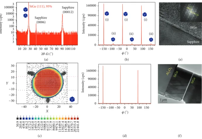
substrate was characterized by several XRD methods devel-oped by NASA Langley. The vertical atomic alignment was measured with a symmetric 2𝜃-Ω scan, which probes the sur-face normal direction. The prominent SiGe (111) peak at2𝜃 ∼ 27.5∘, which appears next to the sapphire (0006) and (00012) peaks, shows[111] oriented SiGe. The horizontal atomic alig-nment is measured with phi (𝜙) scan of the SiGe (220) peaks. Three strong peaks in the𝜙 scan indicate the majority single crystalline SiGe and three small peaks indicate the 60∘rotated SiGe twin crystal.
Phi (𝜙) Scan Method [10]. When the sample is tilted by angle
𝜒, the sample normal 𝑛 is tilted by angle 𝜒 with respect to the 𝑧-axis of the XRD goniometer. This situation is indicated in
Figure 1. For example, when we grow SiGe (111) on𝑐-plane sapphire (0001), the growth direction is aligned to[111] = 𝑛, while the asymmetric SiGe (220) planes are contained on the green plane with the angle𝜒 = 𝛽 = 35.264∘, which is the interplanar angle between (111) and (220) planes of SiGe. If we consider all of the{220} planes of the single crystal SiGe, there will be a total of 12 planes. However, 6 of these are located at the backside of the substrate, while the three planes, (02-2), (20-2), and (2-20), are oriented 90∘with respect to the sample normal[111] and hence do not diffract X-rays. Only the three planes, (022), (202), and (220), strongly diffract. When SiGe layer contains twin defects comprised of both bulk domain and microtwin defects, the defects align as the 60∘ rotated twin crystal along[111]-axis. Therefore, the {220} reflections of twin crystal will be 60∘off in the𝜙 plane from the original crystal’s{220} reflections. The twin crystal’s {220} reflections are now shown as blue dots inFigure 1. Therefore, the𝜙 scan with the angle𝜒 = 𝛽 = 35.264∘shows the{220} peaks from both the original crystal and the 60∘rotated twin crystal.
The𝑦-axis is plotted in a log-scale and the twin crystal’s peak is very weak compared with the majority single crystal’s peak. And the untilted symmetric phi scan of SiGe {440} reflections shows three strong single crystal peaks and three weak twin defect peaks. By setting the sample’s azimuthal𝜙 angle to the desired peak (one of the strong single crystal peaks or one of the weak twin defect peaks) and translating the wafer in the𝑋 and 𝑌 directions, we obtain the 𝑋-𝑌 map-ping image of the SiGe film on𝑐-plane sapphire wafer. The majority single crystal map shows a uniformly strong signal over the entire wafer surface with a small concentrated region of twin defects at the edge. The twin defects on edge were developed due to both the shadow by the wafer holder and the temperature gradient at the edge.
Atomic force microscope (AFM) measurements show the surface topographic variation and root mean square (rms) roughness of the SiGe layer. The crystal structure and layer thickness of the SiGe thin film were characterized using TEM
(0000) K-vector of X-ray Measurement point Twin defect’s (220) Single crystal’s (220) Angle𝜒 120∘ Angle𝜙 2𝜃 Ω(∼𝜃) 𝜒 = 𝛽 → n → Z
Figure 1: Phi (𝜙) scan with tilted 𝜒 for twin crystal detection.
Table 1: Etchant composition for etch-pit density tests and its effects.
Etch Composition (Mol %) Results on{100}
Solvent∗ HF Oxidizer∗∗ Line defects “Point” defects
Secco 67.6 32.2 0.17 Pits Shallow pits or hillocks
Sirtl 71.2 26.3 2.5 Pits or mounds —
Wright 78.5 16.1 5.4 Pits Shallow pits
Seiter 78.5 5.9 15.6 Mounds Mounds
∗H
2O + CH3COOH (HAc);∗∗CrO3+ HNO3.
(FEI, Tecnai G2 F30, 300 KV). The room temperature elec-tron mobilities and carrier densities of the SiGe films were measured using the Hall effect measurement system. To obt-ain reproducible results, the films were cut into several pieces of a standard sized square. Each corner of the square-cut SiGe film with specific doping concentration was soldered onto the four arms of the sample test platform to ensure ohmic contacts. The ohmic contacts can be also checked during the measurement process of Hall mobility.
To reveal the crystalline defects on fab silicon wafer, some chemical etching methods such as Wright [11], SECCO [12], Sirtl [13], and Dash [14] etches have been widely used in failure analysis of semiconductor. SECCO etch is a very useful chemical etching method for the characterization of defects on surface of bare silicon wafer [15].
SECCO etch uses an etchant composition of sol-vent, hydrofluoric acid (HF), and K2Cr2O7 oxidizer as tab-ulated in Table 1. SECCO etch compositions are as follows [12]: hydrofluoric acid (HF), 67% by volume, and 0.15 M K2Cr2O7in H2O, 33% by volume. When mixing the solution, 14.52 g of K2Cr2O7 should be dissolved in 330 mL of H2O. Then, the K2Cr2O7 solution is poured into 670 mL of HF. After mixing, the total volume of the solution is kept in plastic chemical bottle. The defect area is under higher stress; hence, it will etch more quickly in SECCO etchant than the bulk semiconductor. In most of the cases, the result appears as an elliptical pit on substrate at the location of the defect. Optical microscopy is performed to inspect the crystalline defects pitted by SEC-CO etch.
3. Results and Discussion
Figure 2shows the quality of crystalline SiGe film on𝑐-plane sapphire through TEM and XRD. XRD normal scan data shows very strong SiGe (111) peak (Figure 2(a)). In order to check the distribution of SiGe crystal in azimuthal in-plane angles, we used the phi scan method for SiGe{220} peaks and sapphire {10–14} peaks. The phi scan of SiGe {220} peaks shows a large difference in alignment and ratio of majority single crystal. The majority peaks and minority primary-twin peaks that are rotated by 60∘ are noted as (i) and (ii) in Figure 2(b), respectively. The area ratio of the peaks is 95 : 5. In the mapping, a point X-ray source with a 5 nm beam mask was used: (c) shows that almost complete single crystalline SiGe layer was fabricated on the basal plane of trigonal sapphire. Three {10–14} peaks show the trig-onal space symmetry of a sapphire crystal (Figure 2(d)). From the SAED pattern in the upper inset of Figure 2(e), the epitaxial relationship between majority SiGe film and sapphire substrate was found to be(111)SiGe//(0001)sapphire and[-112]SiGe//[01-10]sapphire. These results demonstrate that the[111]-oriented rhombohedral heterostructure epitaxy of a cubic single crystalline SiGe layer on trigonal 𝑐-plane sapphire has been achieved. The SiGe layer was grown in layer-by-layer mode with few micrometers of thicknesses and a smooth interface (Figure 2(f)).
The charge mobility in semiconductor materials is deter-mined and limited by several factors, such as alloy composi-tion, interface roughness, interface charge scattering, lattice
0 50 100 150 0 10000 40000 90000 160000 In te n si ty (c ps) SiGe Sapphire 10 20 30 40 50 60 70 80 90 100110 3 1 3 103 1003 10003 100003 1000003 In te n si ty (c ps) SiGe (111), 95% Sapphire (0006) Sapphire (a) (b) (e) (00012) (i) (i) (ii) (i) (ii) (ii) −150 −100 −50 0 50 100 150 0 10000 40000 90000 160000 In te n si ty (c ps) (d) (f) (c) −150 −100 −50 𝜙 (∘) 𝜙 (∘) 1–11 0003 −2110 220 Al2 O3 SiG e SiG e 1 𝜇m 0 20 40 0 10 20 30 50.9 203.6 458.0 814.2 1 272.2 1832.0 2493.5 3256.9 4122.0 5088.8 6157.5 7327.9 8600.1 9974.1 11 449.9 13 027.4 14 706.8 16 487.9 18 370.7 20 355.4 22 441.8 −10 −20 −30 −40 −20 Y X (∘) 2𝜃-Ω
Figure 2: Analysis of the 95% single crystal SiGe film. Plot (a) shows𝜃-2𝜃 scan in the direction normal to the surface, graph (b) shows phi scan of SiGe peaks for the relative atomic alignment, (c)𝑋-𝑌 wafer mapping with majority {440} peak shows the distribution of a single crystal, (d) shows phi scan of sapphire{10–14} peaks for relative atomic alignment, (e) shows HRTEM and its SAED result of the SiGe (green)/sapphire (yellow) interface, and (f) shows low magnification TEM image after the ion milling process.
mismatch or segregation, and strain relaxation of strained SiGe layers with large Ge content and layer width, as dis-cussed in a recent review by Whall and Parker (2000) [18]. The results by Hall effect measurements indicate that the density of twin lattices is correlated with the electron mobility in the SiGe films.Figure 3(a)shows the calculated electron mobility for relaxed SiGe alloys as a function of their Ge content. As shown inFigure 3(a), relaxed SiGe alloys exhibit drastic decline in mobility mainly due to alloy interface scattering in dislocation populated polycrystal region, except for varying high Ge content (>0.85), where they start behaving like Ge [16,17]. InFigure 3(a), the left side𝑦-axis indicates the pure Si with𝜇𝑛,Si= 1,400 cm2/V⋅s and the right side 𝑦-axis the pure Ge with𝜇𝑛,Ge= 4,000 cm2/V⋅s [19,20]. When epitaxial layer is grown on Si or Ge substrate, in either case alloy composition from pure Si or pure Ge lowers the electron carrier mobility rapidly and they often become polycrystal with many defects in the middle SiGe composition. In spite of the high mobility of Ge, the mobility of SiGe layer is substantially lowered due to the formation of strain caused dislocation defects. The strain caused dislocation defects occur mainly due to the lattice mismatch between Si whose lattice constant is 5.431 ˚A and Ge with 6.657 ˚A [21]. However, if a substrate
allows growing a lattice-matched SiGe layer on it, these defect formation problems can be avoided and the mobility can be drastically enhanced beyond that of Si. Of course, not only is the growth of lattice-matched SiGe layer guaranteed by the crystal symmetry of substrate, but also the growth conditions, such as epilayer speed, substrate temperature, and pressure of processing gases, will dictate the formation of lattice-matched crystalline structures. We observed that the electron mobility is also strongly correlated with the dopant electron density. In Figure 3(b), we figured out the dependence of room temperature electron mobilities on defect density and dopant density in SiGe films. The measured dopant electron densities in three SiGe films are 2.21 × 10¹⁷/cm3, 6.02 × 10¹⁷/cm3, and 1.46 × 10¹⁸/cm3. On the other hand, the defect density measurements were made by the XRD phi scan. The electron mobilities of the tested samples are between those of single crystal Si (𝜇𝑛,Si = 1,400 cm2/V⋅s) and Ge (𝜇𝑛,Ge= 4,000 cm2/V⋅s). The measured electron mobility of a 95% single crystal SiGe was 1538 cm2/V⋅s which is between 350 cm2/V⋅s (Si) and 1550 cm2/V⋅s (Ge) at 6.02 × 10¹⁷/cm3 dopant concentration. And the electron mobility of 99.5% single crystal SiGe is 1552 cm2/V⋅s at the 6.02 × 10¹⁷/cm3 dopant concentration. Figure 3(a) shows that the room
Polycrystal 100% Si 100% Ge Disl ocatio n Dislo catio n 4000 3000 2000 1000 0 0 20 40 60 80 100 Ge contentx (%) Electr o n m o b ili ty 𝜇n (cm 2/V ·s) (a) 0 1 2 3 4 5 6 600 800 1000 12001400 1600 1800 2000 2200 TMs (%) 0.2 0.40.6 0.8 1.0 1.2 1.4 1.6 Electr on de nsity (/cm 3 ) Electr on m ob ility (cm 2/Vs) ×1018 (b)
Figure 3: (a) Calculated phonon-limited 300 K electron low-field mobility in relaxed Si1−𝑥Ge𝑥alloys. Results with (circle) and without (triangle) the inclusion of alloy scattering are shown [16,17]. (b) Three pairs in three-dimensional (3D) plot for room temperature electron mobilities in SiGe films as a function of twin density (TM) and dopant concentration. Red and blue dots show the data points for 99.5% and 95% single crystal SiGe samples grown on𝑐-plane sapphire substrates, respectively.
0 0.25 0.50 0.75 1.00 0 0.25 0.50 0.75 1.00 (𝜇m) 7.0 3.5 0.0 (nm) (a) 0 0.25 0.50 0.75 1.00 Section analysis 4.50 0 4.50 (nm) Surface distance Horizontal distance (L) Vertical distance Angle 21.489 nm 21.484 nm 0.316 nm 0.842∘ (b)
Figure 4: AFM image of SiGe layer on𝑐-plane sapphire: (a) 1 𝜇m × 1 𝜇m area of a SiGe and (b) line profile of cross-section measured along the dark line in (a).
temperature electron mobility in the SiGe films grown on sapphire substrates becomes slightly higher as defect densities are decreased.
Since the topographical and morphological properties of the layer directly influence the charge carrier properties and the channel carrier transport characteristic of the device, the layer needs to be flat in atomic level. The SiGe layer shows a root mean square (rms) roughness of 2 nm for1×1 𝜇m2scan. The AFM analysis shows that the epitaxial layer grows in a layer-by-layer growth mode [22,23], as shown inFigure 4(a).
Figure 4(b)shows a line scan profile along the line indicated, which was selected to pass through a step. It is important to
control the SiGe composition to reduce the lattice mismatch with the𝑐-plane sapphire, maintain an appropriate molecular beam flux rate to ensure flat smooth layer-by-layer growth, and have 2D layer-by-layer growth in electronic microdevice fabrication.
Fine and delicate growth control of SiGe epitaxy to allevi-ate crystalline defects is a serious matter that directly affects yield in device fabrication. In particular, the collective effect of threading dislocations (TDs) attributed to performance degradation has been observed when other types of crystal defects exist individually [24]. In MOSFET, interface misfit dislocations (MDs) which extend between the source and
500 𝜇m (a) (b) 0.3 0.4 0.5 0.6 0.7 0.8 0.9 500 1000 1500 2000 Content of Ge (Si1−xGex) TD P et ch-p it den si ty (/cm 2) (c)
Figure 5: Etch-pit test results of (a) typical SiGe on Si(100) wafer with Ge content = 35% and of (b) rhombohedral SiGe on𝑐-plane sapphire with Ge content = 35% (c) threading dislocation etch-pit density of Si1−𝑥Ge𝑥on sapphire substrate based on the Ge content.
the drain may become electrically active, resulting in incr-eased off-state leakage [25]. The electrical impact of stacking faults (SFs) on device operation can be seen as a combination of the individual effects of misfit and TDs. A single SF in the strained Si channel can degrade the device operation at both off- and on-state conditions [26]. SECCO etch is a chemical etching method used to delineath crystalline defects on silicon substrate and SiGe film. When SECCO etch is used directly, crystalline defects are revealed on silicon substrate or SiGe film after 2 minutes at some areas. Industry standard SECCO etch-pit density measurements were performed on a conventional SiGe layer on Si and 95% single crystalline SiGe layers with 35% Ge content on 𝑐-plane sapphire. A typical SiGe layer with 35% Ge content on a Si(100) wafer shows a high density of dislocation line and etch pits (seeFigure 5(a)). On the other hand, the rhombohedral SiGe grown on 𝑐-plane sapphire with 35% Ge composition ratio shows two orders of magnitude less etch pits and no dislocation lines after performing the SECCO etching (see Figure 5). The conventional SiGe on a Si(100) wafer reveals a threading dis-location pit (TDP) density of 3.9× 10⁴/cm2, line defect density of 1.73× 10⁴/cm2, and a lot of cross-hatch patterns as shown in Figure 5(a). The rhombohedral SiGe grown on 𝑐-plane sapphire has only a TD etch-pit density of 1.9× 10²/cm2,
no visible line defects, and no cross-hatch patterns as shown in Figure 5(b). Therefore, the rhombohedral SiGe shows a 200 times less defect density than conventional SiGe on Si(100) wafer under the SECCO etching tests. Conclusively, we confirmed that a new SiGe film growth technique of fully relaxed SiGe alloy layers yields low TD density epitaxially grown on sapphire substrate [27]. The TD etch-pit density of SiGe on sapphire decreases to 800/cm2 as Ge content increases (see Figure 5(c)). The SiGe films with low TDP density, high electron mobility based on the high Ge content like 85%, and smooth surface were grown on𝑐-plane sapphire substrate. These kinds of films are sufficiently qualified for the fabrication of the ultrafast chipsets like bipolar junction tran-sistors.
The SGOI structures are currently fabricated mainly by two methods, layer transfer [28] and Ge condensation [29,
30]. In the layer transfer method, hydrogen implantation is employed in order to separate a thin SiGe layer from graded SiGe substrates. In the Ge condensation method, a SiGe layer with a low Ge concentration grown on a silicon-on-insulator (SOI) substrate is thermally oxidized, where Ge atoms in the SiGe layer are ejected from the oxide interface resulting in a SiGe layer with a high Ge concentration. However, these met-hods require complex processing routines and do not always
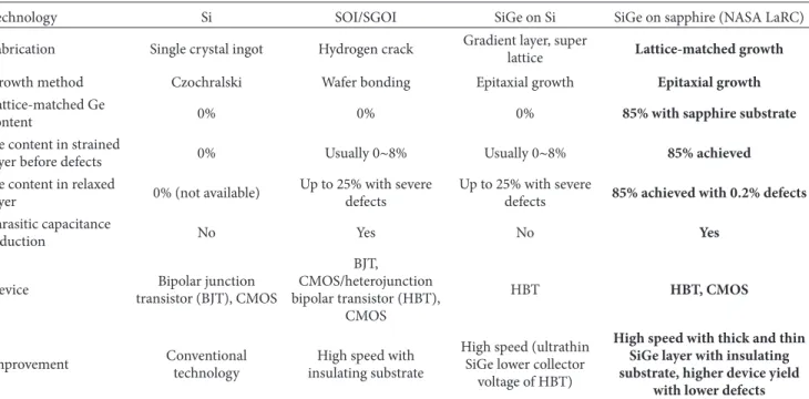
Table 2: Comparison of Si, SOI, and SiGe on Si and LM-SGOI technologies.
Technology Si SOI/SGOI SiGe on Si SiGe on sapphire (NASA LaRC)
Fabrication Single crystal ingot Hydrogen crack Gradient layer, super
lattice Lattice-matched growth
Growth method Czochralski Wafer bonding Epitaxial growth Epitaxial growth
Lattice-matched Ge
content 0% 0% 0% 85% with sapphire substrate
Ge content in strained
layer before defects 0% Usually 0∼8% Usually 0∼8% 85% achieved
Ge content in relaxed
layer 0% (not available)
Up to 25% with severe defects
Up to 25% with severe
defects 85% achieved with 0.2% defects Parasitic capacitance
reduction No Yes No Yes
Device transistor (BJT), CMOSBipolar junction
BJT, CMOS/heterojunction bipolar transistor (HBT), CMOS HBT HBT, CMOS Improvement Conventional technology
High speed with insulating substrate
High speed (ultrathin SiGe lower collector
voltage of HBT)
High speed with thick and thin SiGe layer with insulating substrate, higher device yield
with lower defects
produce high-quality fully relaxed SiGe layer [31]. A different approach reported is an amorphous SiGe layer deposited on SOI substrate and then annealed above the melting point of SiGe after the formation of the SiO2 capping layer [32]. This process has the advantage of simplicity. However, it is difficult to obtain the SiGe layer with high Ge concentration by this process, because the annealing temperature must be reduced below the melting point, resulting in the unusually long annealing time. Rapid thermal annealing (RTA) was also proposed in order to obtain the homogeneous SiGe layer [16]. However, high-quality and uniform SiGe layers were not obtained in the previous study.
We demonstrated the fabrication of high-quality SiGe layers on sapphire substrate by sputtering. The ideal of this process is that a fundamental governing relationship exists in rhombohedral epitaxy process, that is, the growth of ⟨111⟩-oriented cubic crystals on the basal 𝑐-plane of trigonal sapphire crystals [33–35]. One of the concerns with this epi-taxy relationship is that two crystal structures tend to be formed which exhibit a twin lattice structure. This atomic ali-gnment allows polytype crystalline structures with stacking faults on the (111) plane. Rhombohedral alignment, that is, ali-gning the[111] direction of a cubic structure to the [0001] direction of a trigonal structure, can have two possible azim-uthal configurations. Two crystals are twin to each other and they can be formed by a stacking fault during the crystal growth process. We gained an experience to control the amo-unt of the twins based on the growth conditions, especially the growth temperature and deposition power. Our process enables the forming of the SiGe layer of high Ge concentra-tion (85%). For semiconductor device applicaconcentra-tions, high carrier mobility SiGe layers can be made by reducing stacking
faults and microtwin defects. The measurement and control of stacking faults and twin crystals are, therefore, important in the microelectronics applications.
Table 2illustrates the key features of lattice-matched SiGe on insulator (LM-SGOI) currently under development at NASA Langley [36–42] compared to existing products or technologies. The far right column ofTable 2shows the NASA Langley developed SiGe material that is compatible with the conventional insulator silicon oxide. The new rhombohedral epitaxy allows new lattice matching condition of SiGe on sapphire insulator with 85% Ge content and 0.5% defects. While the carrier mobilities of silicon-on-insulator (SOI) are limited by the silicon material, the mobilities of SiGe on 𝑐-plane sapphire can be a few times higher than those of silicon due to the high carrier mobilities of germanium. The silicon-on-sapphire (SOS) became crucial in devices using SOI wafers because sapphire is one of the best insulators. The SOS wafer provides electrically separated regions because of the insulating properties of the sapphire itself, as opposed to other typical devices where the regions are electrically separated using reverse bias between the substrate and device area. The space charge region (carrier depletion region) in the reverse bias case is very thin, in the micrometer range, and the capacitance between a device and the substrate is high and causes the device to have a leakage current at high frequency operating speeds. On the contrary, sapphire is very thick and has an ultrasmall capacitance, thereby reducing parasitic capacitance and leakage currents at high operating frequencies. The lattice-matched SiGe is also complemented by silicon oxide as an insulator and stable gate oxide with SiO2 can make short gate length for RF device. Therefore, RF devices like heterojunction bipolar transistor (HBT) that
are made with rhombohedral SiGe on𝑐-plane sapphire can potentially run a few times faster than RF devices on SOS wafers at high frequencies up to several hundred GHz.
4. Summary and Conclusions
In summary, we have experimentally demonstrated the fab-rication of high-quality SiGe layers with a high Ge concen-tration of more than 85% on sapphire wafer by sputtering. We also report that the defect dependence of the electron mobility by the twinning of SiGe thin films on sapphire (0001) substrates was measured. Currently, a standard SiGe technology uses only ultrathin (30∼100 nm) layer of SiGe for base layer of heterojunction bipolar transistor (HBT) to avoid dislocation defects. With the lattice-matched SiGe layer we developed, a thin or thick SiGe layer can be also fabricated for any designated applications, since the lattice-matched materials do not have a critical thickness limit. In rhombo-hedral SiGe on𝑐-plane (0001) sapphire, the SiGe layer can be also grown in layer-by-layer mode from sub-100 nm to few micrometers of thicknesses. Therefore, thin rhombohedral SiGe on𝑐-plane sapphire has many commercial application potentials as do SOI wafers in addition to solar cell applica-tions. Typically, a rhombohedral single crystal SiGe has 2 or 3 times higher carrier mobility than monocrystalline silicon. The high Ge-content SiGe film shows high mobility, low cost, and simple structure when grown directly on sapphire substrate with sputtering process. If the defects in SiGe can be removed, transistors with higher operational frequencies can be fabricated for a new generation of ultrafast chipsets because of the high mobility of SiGe film.
Conflict of Interests
The authors declare that there is no conflict of interests regarding the publication of this paper.
References
[1] D. L. Harame and B. S. Meyerson, “The early history of IBM’s SiGe mixed signal technology,” IEEE Transactions on Electron Devices, vol. 48, no. 11, pp. 2555–2567, 2001.
[2] C. Gui, M. Elwenspoek, N. Tas, and J. G. E. Gardeniers, “The effect of surface roughness on direct wafer bonding,” Journal of Applied Physics, vol. 85, no. 10, pp. 7448–7454, 1999.
[3] “Semiconductor Wafer edge analysis,” Chapman Technical Note TW-1, 1998.
[4] H. Ahmataku and K. Kipli, in Proceedings of the IEEE Inter-national Conference on Semiconductor Electronics (ICSE ’10), Melaka, Malaysia, June 2010.
[5] I. McMackin, W. Martin, J. Perez et al., “Patterned wafer defect density analysis of step and flash imprint lithography,” Journal of Vacuum Science & Technology B, vol. 26, no. 1, pp. 151–155, 2008. [6] S. A. Alterovitz, C. H. Mueller, and E. T. Croke, “High mobility SiGe/Si transistor structures on sapphire substrates using ion implantation,” Journal of Vacuum Science & Technology B, vol. 22, p. 1776, 2004.
[7] K. Ismail, M. Arafa, K. L. Saenger, J. O. Chu, and B. S. Meyerson, “Extremely high electron mobility in Si/SiGe modulation-doped heterostructures,” Applied Physics Letters, vol. 66, no. 9, pp. 1077–1079, 1995.
[8] S. J. Koester, R. Hammond, J. O. Chu et al., “SiGe pMODFETs on silicon-on-sapphire substrates with 116 GHz fmax,” IEEE Electron Device Letters, vol. 22, no. 2, pp. 92–94, 2001.
[9] W. B. Dubbelday and K. L. Kavanagh, “Growth of SiGe on sap-phire using rapid thermal chemical vapor deposition,” Journal of Crystal Growth, vol. 222, no. 1-2, pp. 20–28, 2001.
[10] Y. Park, H. J. Kim, G. C. King, and S. H. Choi, “X-ray diffraction wafer mapping method for SiGe twin defects characterization,” in Nanosensors, Biosensors, and Info-Tech Sensors and Systems, vol. 7980 of Proceedings of SPIE, April 2011.
[11] M. W. Jenkins, “A new preferential etch for defects in silicon crystals,” Journal of the Electrochemical Society: Solid-State Science and Technology, vol. 124, no. 5, pp. 757–762, 1977. [12] F. Secco d’Aragona, “Dislocation etch for (100) planes in silicon,”
Journal of The Electrochemical Society, vol. 119, no. 7, pp. 948–951, 1972.
[13] E. Sirtl and A. Adler, “Chromic acid-hydrofluoric acid as specific reagents for the development of etching pits in silicon,” Zeitschrift f¨ur Metallkunde, vol. 52, pp. 529–534, 1961.
[14] W. C. Dash, “Copper precipitation on dislocations in silicon,” Journal of Applied Physics, vol. 27, no. 10, pp. 1193–1195, 1956. [15] H. Rauh, Wacker’s Atlas for Characterization of Defects in Silicon,
A Part of the Wacker Tutorial Series, 1986.
[16] M. Glicksman, “Mobility of Electrons in Germanium-Silicon Alloys,” Physical Review, vol. 111, no. 1, pp. 125–128, 1958. [17] M. V. Fischetti and S. E. Laux, “Band structure, deformation
potentials, and carrier mobility in strained Si, Ge, and SiGe alloys,” Journal of Applied Physics, vol. 80, no. 4, pp. 2234–2252, 1996.
[18] T. E. Whall and E. H. C. Parker, “Si/SiGe/Si pMOS performa-nce—alloy scattering and other considerations,” Thin Solid Films, vol. 368, pp. 297–305, 2000.
[19] C. Jacoboni, C. Canali, G. Ottaviani, and A. Alberigi Quaranta, “A review of some charge transport properties of silicon,” Solid State Electronics, vol. 20, no. 2, pp. 77–89, 1977.
[20] V. I. Fistul, M. I. Iglitsyn, and E. M. Omelyanovskii, “Mobility of electrons in germanium strongly doped with arsenic,” Soviet Physics, Solid State, vol. 4, no. 4, pp. 784–785, 1962.
[21] Landolt-B¨ornstein, New Series Group III, vol. 17a, Springer, Berlin, Germany, 1982.
[22] F. C. Frank and J. H. van de Merwe, “One-dimensional disloca-tions. I. Static theory,” Proceedings of the Royal Society of London: Series A, vol. 198, no. 1053, pp. 205–216, 1949.
[23] F. C. Frank and J. H. van de Merwe, “One-dimensional disloca-tions. IV. Dynamics,” Proceedings of the Royal Society of London A, vol. 201, no. 1065, pp. 261–268, 1950.
[24] E. Escobedo-Cousin, S. H. Olsen, A. G. O’Neill, and H. Coulson, “Defect identification in strained Si/SiGe heterolayers for device applications,” Journal of Physics D: Applied Physics, vol. 42, no. 17, Article ID 175306, 2009.
[25] J. G. Fiorenza, G. Braithwaite, C. W. Leitz et al., “Film thickness constraints for manufacturable strained silicon CMOS,” Semi-conductor Science and Technology, vol. 19, no. 1, article L4, 2004. [26] J. N. Yang, G. W. Neudeck, and J. P. Denton, “Electrical effects of a single stacking fault on fully depleted thin-film silicon-on-insulator P-channel metal-oxide-semiconductor field-effect
transistors,” Journal of Applied Physics, vol. 91, no. 1, pp. 420– 426, 2002.
[27] P. I. Gaiduk, A. Nylandsted Larsen, and J. Lundsgaard Hansen, “Strain-relaxed SiGe/Si heteroepitaxial structures of low threading-dislocation density,” Thin Solid Films, vol. 367, no. 1-2, pp. 120–125, 2000.
[28] L. J. Huang, J. O. Chu, D. F. Canaperi et al., “SiGe-on-insulator prepared by wafer bonding and layer transfer for high-perfor-mance field-effect transistors,” Applied Physics Letters, vol. 78, no. 9, pp. 1267–1269, 2001.
[29] T. Tezuka, N. Sugiyama, T. Mizuno, M. Suzuki, and S. Takagi, “A novel fabrication technique of ultrathin and relaxed SiGe buffer layers with high Ge fraction for Sub-100 nm strained silicon-on-insulator MOSFETs,” Japanese Journal of Applied Physics, vol. 40, part 1, no. 4B, pp. 2866–2874, 2001.
[30] S. Nakaharai, T. Tezuka, N. Sugiyama, Y. Moriyama, and S.-I. Takagi, “Characterization of 7-nm-thick strained Ge-on-insulator layer fabricated by Ge-condensation technique,” Applied Physics Letters, vol. 83, no. 17, pp. 3516–3518, 2003. [31] T. Shimura, K. Kawamura, M. Asakawa et al., “Characterization
of strained Si wafers by X-ray diffraction techniques,” Journal of Materials Science: Materials in Electronics, vol. 19, no. 1, supplement, pp. S189–S193, 2008.
[32] N. Sugii, S. Yamaguchi, and K. Washio, “SiGe-on-insulator substrate fabricated by melt solidification for a strained-silicon complementary metal–oxide–semiconductor,” Journal of Vac-uum Science & Technology B, vol. 20, no. 5, pp. 1891–1896, 2002. [33] H.-J. Kim, H.-B. Bae, Y. Park, K. Lee, and S. H. Choi, “Tempera-ture dependence of crystalline SiGe growth on sapphire (0001) substrates by sputtering,” Journal of Crystal Growth, vol. 353, no. 1, pp. 124–128, 2012.
[34] Y. Park, G. C. King, and S. H. Choi, “Rhombohedral epitaxy of cubic SiGe on trigonal c-plane sapphire,” Journal of Crystal Gro-wth, vol. 310, no. 11, pp. 2724–2731, 2008.
[35] H. J. Kim, H. B. Bae, Y. Park, and S. H. Choi, “Defect-engineered Si1−𝑥Ge𝑥 alloy under electron beam irradiation for thermoelectrics,” RSC Advances, vol. 2, no. 33, pp. 12670– 12674, 2012.
[36] Y. Park, S. H. Choi, and G. C. King, “Silicon germanium semi-conductive alloy and method of fabricating same,” US Patent no. 7,341,883, 2008.
[37] Y. Park, S. H. Choi, G. C. King, J. R. Elliott Jr., and D. M. Stoakley, “Graded index silicon geranium on lattice matched silicon geranium semiconductor alloy,” US Patent No. 7514726 B2, 2009.
[38] Y. Park, S. Hyouk Choi, G. C. King, and J. R. Elliott, “Method of generating X-ray diffraction data for integral detection of twin defects in super-hetero-epitaxial materials,” US Patent no. 7,558,371 B2, 2009.
[39] Y. Park, S. H. Choi, and G. C. King, “Epitaxial growth of cubic crystalline semiconductor alloys on basal plane of trigonal or hexagonal crystal,” US Patent no. 7,906,358 B2, 2011.
[40] T. Maniwa, “Steering apparatus,” US Patent No. 8,826,767, 2012. [41] Y. Park, S. H. Choi, G. C. King, and J. R. Elliott, “Rhombohedral cubic semiconductor materials on trigonal substrate with single crystal properties and devices based on such materials,” US Patent no. 8,257,491 B2, 2012.
[42] Y. Park, S. H. Choi, G. C. King, J. R. Elliott, and A. L. Dimarcan-tonio, “X-ray diffraction wafer mapping method for rhombohe-dral super-hetero-epitaxy,” US Patent No. 7769135 B2, 2010.
Submit your manuscripts at
http://www.hindawi.com
Hindawi Publishing Corporation
http://www.hindawi.com Volume 2014 High Energy PhysicsAdvances in
http://www.hindawi.com Volume 2014
Hindawi Publishing Corporation
http://www.hindawi.com Volume 2014
Fluids
Journal ofAtomic and Molecular Physics Journal of
Hindawi Publishing Corporation
http://www.hindawi.com Volume 2014 http://www.hindawi.com Volume 2014
Optics
International Journal of Hindawi Publishing Corporationhttp://www.hindawi.com Volume 2014
Hindawi Publishing Corporation
http://www.hindawi.com Volume 2014
Astronomy
Advances inInternational Journal of Hindawi Publishing Corporation
http://www.hindawi.com Volume 2014
Superconductivity
Hindawi Publishing Corporationhttp://www.hindawi.com Volume 2014
Statistical Mechanics
International Journal of http://www.hindawi.com Volume 2014
Hindawi Publishing Corporation
http://www.hindawi.com Volume 2014
Astrophysics
Journal ofHindawi Publishing Corporation
http://www.hindawi.com Volume 2014 Physics
Research International
Hindawi Publishing Corporation
http://www.hindawi.com Volume 2014 Solid State PhysicsJournal of Computational Methods in Physics
Journal of
Hindawi Publishing Corporation
http://www.hindawi.com Volume 2014
http://www.hindawi.com Volume 2014
Hindawi Publishing Corporation http://www.hindawi.com
Aerodynamics
Journal ofVolume 2014 http://www.hindawi.com Volume 2014
Hindawi Publishing Corporation
http://www.hindawi.com Volume 2014
Journal of
Biophysics
Hindawi Publishing Corporationhttp://www.hindawi.com Volume 2014