Mode junction photonics with a
symmetry-breaking arrangement of mode-orthogonal
heterostructures
Sunkyu Yu,1 Xianji Piao,1 Sukmo Koo,1 Jung H. Shin,2 Seung Hoon Lee,3 Bumki Min,3 and Namkyoo Park1,*
1Photonic Systems Laboratory, School of EECS, Seoul National Univ., Seoul 151-744, South Korea 2Dept. of Phys. / Graduate School of Nanoscience and Technology, KAIST, Daejeon, South Korea
3
Micro/Nano Photonics Lab., Dept. of Mech. Eng., KAIST, Daejeon, South Korea *nkpark@snu.ac.kr
Abstract: Junction structures provide the foundation of digital electronics and spintronics today. An equivalent, a photonic junction to achieve systematic and drastic control of photon flow is currently missing, but is mandatory for serious all-optical signal processing. Here we propose a photonic junction built upon mode-orthogonal hetero-structures, as a fundamental structural unit for photonic integrated circuits. Controlling the optical potential of mode-orthogonal junctions, the flow of photons can be dynamically manipulated, to complete the correspondence to the electronic junction structures. Of the possible applications, we provide examples of a photonic junction diode and a multi-junction half-adder, with exceptional performance metrics. Highly directional (41dB), nearly unity throughput, ultra-low threshold-power, high quality signal regeneration at 200Gb/s, and all-optic logic operations are successfully derived with the self-induced, bi-level dynamic mode-conversion process across the junction.
©2011 Optical Society of America
OCIS codes: (130.3120) Integrated optics devices; (200.4660) Optical logic; (230.4320)
Nonlinear optical devices; (230.4555) Coupled resonators; (230.5298) Photonic crystals.
References and links
1. C. Koos, P. Vorreau, T. Vallaitis, P. Dumon, W. Bogaerts, R. Baets, B. Esembeson, I. Biaggio, T. Michinobu, F. Diederich, W. Freude, and J. Leuthold, “All-optical high-speed signal processing with silicon–organic hybrid slot waveguides,” Nat. Photonics 3(4), 216–219 (2009).
2. G. Lenz, J. Zimmermann, T. Katsufuji, M. E. Lines, H. Y. Hwang, S. Spälter, R. E. Slusher, S. W. Cheong, J. S. Sanghera, and I. D. Aggarwal, “Large Kerr effect in bulk Se-based chalcogenide glasses,” Opt. Lett. 25(4), 254– 256 (2000).
3. S. Tatsuura, M. Furuki, Y. Sato, I. Iwasa, M. Tian, and H. Mitsu, “Semiconductor carbon nanotubes as ultrafast switching materials for optical telecommunications,” Adv. Mater. (Deerfield Beach Fla.) 15(6), 534–537 (2003). 4. M. Hochberg, T. Baehr-Jones, G. Wang, M. Shearn, K. Harvard, J. Luo, B. Chen, Z. Shi, R. Lawson, P. Sullivan,
A. K. Y. Jen, L. Dalton, and A. Scherer, “Terahertz all-optical modulation in a silicon-polymer hybrid system,” Nat. Mater. 5(9), 703–709 (2006).
5. V. R. Almeida, C. A. Barrios, R. R. Panepucci, and M. Lipson, “All-optical control of light on a silicon chip,” Nature 431(7012), 1081–1084 (2004).
6. M. Soljačić and J. D. Joannopoulos, “Enhancement of nonlinear effects using photonic crystals,” Nat. Mater.
3(4), 211–219 (2004).
7. K. Nozaki, T. Tanabe, A. Shinya, S. Matsuo, T. Sato, H. Taniyama, and M. Notomi, “Sub-femtojoule all-optical switching using a photonic-crystal nanocavity,” Nat. Photonics 4(7), 477–483 (2010).
8. B. Min, E. Ostby, V. Sorger, E. Ulin-Avila, L. Yang, X. Zhang, and K. Vahala, “High-Q surface-plasmon-polariton whispering-gallery microcavity,” Nature 457(7228), 455–458 (2009).
9. J. A. Schuller, E. S. Barnard, W. Cai, Y. C. Jun, J. S. White, and M. L. Brongersma, “Plasmonics for extreme light concentration and manipulation,” Nat. Mater. 9(3), 193–204 (2010).
10. J. B. Khurgin, “Optical buffers based on slow light in electromagnetically induced transparent media and coupled resonator structures: comparative analysis,” J. Opt. Soc. Am. B 22(5), 1062–1074 (2005).
11. F. Leo, S. Coen, P. Kockaert, S. Gorza, P. Emplit, and M. Haelterman, “Temporal cavity solitons in one-dimensional Kerr media as bits in an all-optical buffer,” Nat. Photonics 4(7), 471–476 (2010).
12. M. F. Yanik, S. Fan, M. Soljacić, and J. D. Joannopoulos, “All-optical transistor action with bistable switching in a photonic crystal cross-waveguide geometry,” Opt. Lett. 28(24), 2506–2508 (2003).
13. P. L. Li, D. X. Huang, X. L. Zhang, and G. X. Zhu, “Ultrahigh-speed all-optical half adder based on four-wave mixing in semiconductor optical amplifier,” Opt. Express 14(24), 11839–11847 (2006).
14. Q. Liu, Z. Ouyang, C. J. Wu, C. P. Liu, and J. C. Wang, “All-optical half adder based on cross structures in two-dimensional photonic crystals,” Opt. Express 16(23), 18992–19000 (2008).
15. S. Yu, S. Koo, and N. Park, “Coded output photonic A/D converter based on photonic crystal slow-light structures,” Opt. Express 16(18), 13752–13757 (2008).
16. R. Slavík, F. Parmigiani, J. Kakande, C. Lundstro¨m, M. Sjo¨din, P. A. Andrekson, R. Weerasuriya, S. Sygletos, A. D. Ellis, L. Gru¨ner-Nielsen, D. Jakobsen, S. Herstrøm, R. Phelan, J. O’Gorman, A. Bogris, D. Syvridis, S. Dasgupta, P. Petropoulos, and D. J. Richardson, “All-optical phase and amplitude regenerator for next-generation telecommunications systems,” Nat. Photonics 4(10), 690–695 (2010).
17. L. Liu, R. Kumar, K. Huybrechts, T. Spuesens, G. Roelkens, E.-J. Geluk, T. de Vries, P. Regreny, D. Van Thourhout, R. Baets, and G. Morthier, “An ultra-small, low-power, all-optical flip-flop memory on a silicon chip,” Nat. Photonics 4(3), 182–187 (2010).
18. Y. J. Jung, C. W. Son, Y. M. Jhon, S. Lee, and N. Park, “One-level simplification method for all-optical combinational logic circuits,” IEEE Photon. Technol. Lett. 20(10), 800–802 (2008).
19. J. H. Scaff and R. S. Ohl, “Development of silicon crystal rectifiers for microwave radar receivers,” Bell Syst. Tech. J. 26, 1–30 (1947).
20. S. A. Wolf, D. D. Awschalom, R. A. Buhrman, J. M. Daughton, S. von Molnár, M. L. Roukes, A. Y. Chtchelkanova, and D. M. Treger, “Spintronics: a spin-based electronics vision for the future,” Science
294(5546), 1488–1495 (2001).
21. A. A. Tulapurkar, Y. Suzuki, A. Fukushima, H. Kubota, H. Maehara, K. Tsunekawa, D. D. Djayaprawira, N. Watanabe, and S. Yuasa, “Spin-torque diode effect in magnetic tunnel junctions,” Nature 438(7066), 339–342 (2005).
22. K. Gallo, G. Assanto, K. R. Parameswaran, and M. M. Fejer, “All-optical diode in a periodically poled lithium niobate waveguide,” Appl. Phys. Lett. 79(3), 314–316 (2001).
23. S. F. Mingaleev and Y. S. Kivshar, “Nonlinear transmission and light localization in photonic-crystal waveguides,” J. Opt. Soc. Am. B 19(9), 2241–2249 (2002).
24. R. Philip, M. Anija, C. S. Yelleswarapu, and D. V. G. L. N. Rao, “Passive all-optical diode using asymmetric nonlinear absorption,” Appl. Phys. Lett. 91(14), 141118 (2007).
25. N. Zhao, H. Zhou, Q. Guo, W. Hu, X. Yang, S. Lan, and X. Lin, “Design of highly efficient optical diodes based on the dynamics of nonlinear photonic crystal molecules,” J. Opt. Soc. Am. B 23(11), 2434–2440 (2006). 26. X. S. Lin, W. Q. Wu, H. Zhou, K. F. Zhou, and S. Lan, “Enhancement of unidirectional transmission through the
coupling of nonlinear photonic crystal defects,” Opt. Express 14(6), 2429–2439 (2006).
27. V. Grigoriev and F. Biancalana, “Nonreciprocal switching thresholds in coupled nonlinear microcavities,” Opt. Lett. 36(11), 2131–2133 (2011).
28. Z. Yu and S. Fan, “Complete optical isolation created by indirect interband photonic transitions,” Nat. Photonics
3(2), 91–94 (2009).
29. G. P. Agrawal, Fiber-Optic Communication Systems (John Wiley & Sons, 2002).
30. J. Hwang, M. H. Song, B. Park, S. Nishimura, T. Toyooka, J. W. Wu, Y. Takanishi, K. Ishikawa, and H. Takezoe, “Electro-tunable optical diode based on photonic bandgap liquid-crystal heterojunctions,” Nat. Mater.
4(5), 383–387 (2005).
31. A. Taflove and S. C. Hagness, Computational Electrodynamics: The Finite-Difference Time-Domain Method (Artech House, 2000).
32. X. Hu, Q. Zhang, Y. Liu, B. Cheng, and D. Zhang, “Ultrafast three-dimensional tunable photonic crystal,” Appl. Phys. Lett. 83(13), 2518–2520 (2003).
33. M. Soljačić, M. Ibanescu, S. G. Johnson, Y. Fink, and J. D. Joannopoulos, “Optimal bistable switching in nonlinear photonic crystals,” Phys. Rev. E Stat. Nonlin. Soft Matter Phys. 66(5), 055601 (2002). 34. J. S. Aitchison, D. C. Hutchings, J. U. Kang, G. I. Stegeman, and A. Villeneuve, “The Nonlinear Optical
Properties of AlGaAs at the Half Band Gap,” IEEE J. Quantum Electron. 33(3), 341–348 (1997).
35. X. Hu, P. Jiang, C. Ding, H. Yang, and Q. Gong, “Picosecond and low-power all-optical switching based on an organic photonic-bandgap microcavity,” Nat. Photonics 2(3), 185–189 (2008).
36. R. W. Boyd, Nonlinear Optics (Academic Press, 1992).
37. E. Kuramochi, M. Notomi, S. Mitsugi, A. Shinya, T. Tanabe, and T. Watanabe, “Ultrahigh-Q photonic crystal nanocavities realized by the local width modulation of a line defect,” Appl. Phys. Lett. 88(4), 041112 (2006). 38. H. A. Haus, Waves and Fields in Optoelectronics (Prentice-Hall, 1984).
39. C. Manolatou, M. J. Khan, S. Fan, P. R. Villeneuve, H. A. Haus, and J. D. Joannopoulos, “Coupling of modes analysis of resonant channel add-drop filters,” IEEE J. Quantum Electron. 35(9), 1322–1331 (1999). 40. T. Uesugi, B. S. Song, T. Asano, and S. Noda, “Investigation of optical nonlinearities in an ultra-high-Q Si
nanocavity in a two-dimensional photonic crystal slab,” Opt. Express 14(1), 377–386 (2006).
1. Introduction
The ultrafast, distortion-free optical communication of today owes its remarkable success in large part to the time-reversal symmetry of Maxwell’s equations and the charge-less nature of photons, that providing untainted linearity for optical materials and devices. Still at the same time, this very linearity has seriously hindered the development of photonic logic devices or systems. Nonlinearity being the core in the realization of logic devices, serious effort is now
in progress to enhance the nonlinearity. Various nonlinear materials [1–4], means of field enhancement [5–9], functional elements [10–12], signal processors [13–17], and photonic-specific circuit design algorithms [18] have been suggested to fully exploit the photonic bandwidth advantage, and to fulfill the promise of all-optical signal processing.
Notwithstanding past effort, attempting the success of digital photonics is still in an early stage, with their premature performances. Worth to examine at this phase of stall would be the breakthrough of electronics, especially witnessed after the introduction of junction structures.
Providing drastic, systematic and controllable change to the asymmetric electrical potential
(or spin orientation) across [19–21], the junction has enabled highly advanced, non-reciprocal and nonlinear manipulation for the transport of electrons - the core attributes in the realization of diode, transistor, and logic processors in the electronics / spintronics of today.
Here, taking photonics as an example, we propose a junction for wave, built upon mode-orthogonal photonic hetero-structures, as a fundamental structural unit for ‘photo-tronics’. By exploiting the rich and well-defined orthogonal modes which provide abundant degrees of freedom for the choice of junctions (having different spectral mode-overlap and frequency separation), the modular construction of highly nonlinear devices with systematic control of wave propagation is enabled. Of possible applications for the mode junction, here we provide examples of a photonic junction diode and a multi-junction half-adder, of exceptional performance metrics. Highly directional (41dB), nearly unity throughput with orders of magnitude lower threshold power (~103, compared to [22–28]. For [28], external modulation power), a high quality signal regeneration [16,29] at 200Gb/s, and all-optical AND, XOR operations are successfully demonstrated.
2. Mode junction - principles
To incorporate the junction structure into the photonic domain - notwithstanding the absence of charge or reference energy, we focus our attention to the wave nature of photons; especially related to the orthogonality between their well-defined and plentiful eigenmodes. Through the juxtaposition of two photonic structures of each supporting different eigenmodes, a diversity of mode-orthogonal heterojunctions can be created. Explicitly, exploiting the abundant set of optical eigenmodes (~Na · Nm · Np where Ni = mode number for optical atom, molecule, and polarization), variety of mode-orthogonal heterojunctions (atomic-, molecular-, polarization junctions as in Fig. 1(a)) can be created, which differ in their mode-overlap and frequency separations. To note, without loss of generality but with the ease of implementation, and also considering the range of operation frequencies, from now on we use the molecular junctions constructed of multi-atomic structures (Fig. 1(b)).
For example, let us consider the a junction juxtaposed of two structures (Fig. 1(c)), each supporting T- (1, 2, 1) and T0 (- 2, 0, 2) modes of tri-atomic resonator (the eigenvector component represents the field amplitude of each atom), at the operation frequency. By adjusting the permittivity (optical potential) for a specific region (here, left side of the junction), the dominant eigenmode at the operation frequency of the controlled region then can be dynamically switched between T- and T0, to block (<T- / T0> = 0) or to authorize (<T0 / T0> = 1) the transmission of photons across the junction structure. To note, now onwards we denote; / j > as the eigenmode of the structure, Ψi-j as the potential-controlled region -
supporting mode / i > in unbiased state (Fig. 1(c) in yellow), but toggling to / j > with shifted optical potential (pink in Fig. 1(c)) either by external excitation or self-induced manner.
Fig. 1. (a) Examples of orthogonal mode junctions constructed between two orthogonal modes, providing different frequency separation and modal overlap properties. (b) Examples of molecular modes, which could be used to construct a variety of molecular mode junction (S, D, T: Single-, Di-, Tri- atomic molecular modes). A T- / T0 mode junction, for example, can be constructed between two structures providing orthogonal modes of T- and T0 (composed of optical atoms in single mode, sharing an identical polarization). Dashed circles in Fig. 1(a) and 1(b) represent optical atoms. (c) Operation principles of the mode junction. Excited modes at the operation frequency are marked with filled curves. NT-(E) and NT0(E) axis represents the
density of states for T- and T0 mode. Adjusting the optical potential, the dominant mode of the controlled region can be switched between T- (non-shifted, yellow) and T0 (potential ∆E-shifted, pink) modes, to give a junction throughput of either a ‘0’ (yellow) or ‘1’ (pink). The coupling across the junction is determined by the inner product between eigenmodes of the left/right structures (equivalently, multiplying spatial mode profiles at the same frequency along the identical mode axis (T- or T0)).
3. Application I – photonic junction diode: principles
Out of the many possible functional devices that a junction can enable, we first consider the case of the photonic diode. For an electrical diode [19] especially being highly nonlinear and asymmetric in its response providing the key functionality for current flow manipulation, its photonic counterpart, the photonic diode [22–28,30], has also attracted serious attention. Nevertheless, for the past demonstrations of photonic diode extremely costly in threshold power (~W/µm), with the added trouble of limited throughput or directionality, it will be of worth to investigate whether the proposed junction structure could provide any advantages.
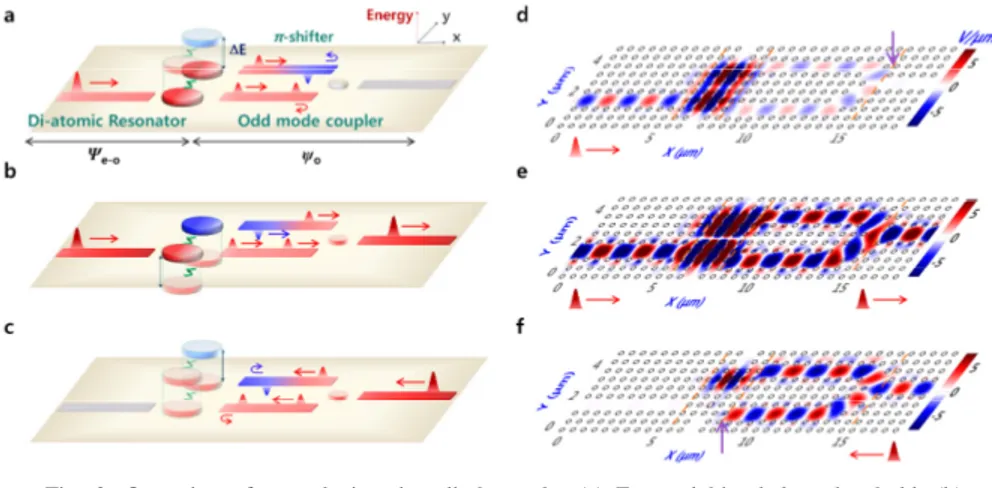
As illustrated in Fig. 2(a)–2(c), without loss of generality, let us consider a di-atomic resonator providing even- and odd- modes, separated in its frequencies (ωe and ωo). At the operation frequency ωe the di-atomic resonator in the even mode forms a ψe-ψo mode junction when combined with the ψo odd-mode coupler (an 1 x 2 splitter and a π phase shifter in one arm). Critical to note, compared to the right-side low-Q ψo coupler, for the left-side high-Q di-atomic resonator enjoying a higher density of photons and thus a much enhanced, self-induced optical nonlinearity, the modification of the optical potential for the Ψe-o-ψo junction becomes strongly dependent on the direction of the incident wave, so as to fulfill the directionality required for diode operation. Specifically, the critical consequences are as follows. First, for the forward bias below threshold (Ψe-ψo, Fig. 2(a)), the wave propagation to the other side of the junction is completely prohibited and reflected, as dictated by the mode orthogonality < e /
o > = 0. Meanwhile, for the forward bias above threshold, with a strong on-resonance (ωe) build-up of the field in the resonator and a corresponding optical potential shift (n2 I / n0 ~(ωo - ωe) / ωc), the dominant mode in the resonator Ψe-o then gets converted from even to odd mode (Ψo-ψo, Fig. 2(b)), to render full transparency to the ψo coupler region (< o / o > = 1). Finally, for the reverse bias (Fig. 2(c)), the coupling from the odd mode coupler to even mode di-atomic resonator is suppressed by the mode orthogonality. In this case, the weakly-excited
resonator will remain in the even mode, blocking the transmission, until the reverse bias reaches the breakdown - determined by the non-zero mode overlap factor (Appendix A).
Fig. 2. Operation of a mode junction diode: under (a) Forward bias below threshold, (b) Forward bias above threshold, and (c) Reverse bias. Corresponding field patterns in the photonic crystal realization are shown in (d) ~(f) (details of numerical analysis in Appendix-A). Unidirectional transmission of the signal is evident only for the state 2(e), confirming the diode operation above threshold. For other states of operation, the wave propagation is inhibited; (d), at the odd-mode coupler for forward bias. (f), at the right end barrier of the di-atomic resonator, for reverse bias.
Meanwhile simple in its principle, the junction diode offers distinctive advantages. First, when compared to past approaches utilizing asymmetric potential barriers for directional operation of the diode (at the expense of severe impedance mismatch, (Fig. 3(e), 1/τL >> 1/τR) [22–26], now for the proposed junction diode, it is possible to keep the full symmetry of the potential barrier - by transferring the required diode directionality to the asymmetric arrangement of mode-orthogonal structures. As a result, an impedance-matched design can be constructed, without any sacrifice in directionality or throughput (Fig. 3(a), 1/τL = 1/τR1 + 1/τR2). Furthermore, with the orthogonal, two-band, on-resonance operation of the Ψe-o-ψo
junction (Fig. 3(b)–3(d), contrast to the expensive off-resonance excitation for single-band diode operation shown in Fig. 3(f)–3(h)), it is possible to simultaneously realize; high reverse breakdown (from mode orthogonality), ultra-low threshold power (from the on-resonance
feeding to the resonator in the even mode, Fig. 3(b)), and near unity throughput (with the
on-resonance releasing of the resonator odd mode, to the ψo mode coupler, as in Fig. 3(c)).
Fig. 3. (a) Impedance matched (1/τL = 1/τR1 + 1/τR2) low reflection design is achieved with a
junction diode, by adjusting τL. (e) Illustration of impedance imbalance, for the case of single
band photonic diode (case of τR = 4τL). Mode-dependent field intensity inside resonators (even:
|a1 + a2|2, odd: |a1-a2|2) for structures in (a) and (e) are shown for; (b) and (f) - forward bias
before threshold, (c) and (g) - forward bias after threshold, (d) and (h) - under reverse bias. For two-band operation (b) at the operation frequency ωop (dashed line), on resonance feeding and
low power excitation of the resonator is achieved. κ = 0.003ωop, and Q = 200.
4. Application I – photonic junction diode: implementation and results
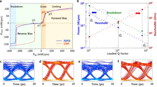
For implementation and demonstration of the proposed idea, without loss of generality, a 2D square-lattice rod-type photonic crystal platform was used (structural details in the Appendix). Of various optical nonlinearities, here we assume the conventional Kerr nonlinearity, to achieve a fair comparison with previous works. For the three states of the diode operation illustrated in Fig. 2(a)–2(c), Fig. 2(d)–2(f) show the corresponding field patterns at the operating frequency ωe of 193.24THz (1551.4nm), obtained from two dimensional Finite Difference Time Domain (2D-FDTD) analysis [31]. It is worth noting that, for the reverse operation (Fig. 2(f)), the mode orthogonality between the odd-coupler impinging wave and di-atomic resonator in the even mode resulted in a much weaker (12dB) energy build-up in the (upper) resonator, when compared to the case of forward bias. By minimizing the spectral overlap between the even and odd mode (Fig. 3(c)), this residual build-up of the field (setting the reverse breakdown point) could be further suppressed. Blue line in Fig. 4(a) also shows the FDTD obtained static response curves of the diode, as a function of input power (+ / - for forward / reverse bias). A threshold as low as 23mW/µm (~103 improvement over [22–28]), and a high reverse breakdown as much as 481mW/µm was observed, confirming the ultra-low power, highly unidirectional operation of the junction diode. The maximum contrast and throughput was found to be 41dB (at 142.2mW/µm. 15.7dB at peak throughput) and 0.96 (at 64.1mW/µm).
Fig. 4. (a) Numerically (FDTD, blue lines, Appendix A), and analytically (CMT, red lines, Appendix B) obtained response curve of the Ψe-o-ψo junction diode. (b) Temporal-CMT
calculated threshold power (blue circle), breakdown power (green circle), and operation bandwidth (red circle) as a function of the loaded Q-factor of a di-atomic resonator. Solid triangles overlaid to the plot are results of the FDTD, obtained with photonic diode realizations of different loaded quality factors Q1 = 1094, Q2 = 10945, and Q3 = 74895 (achieved by
adjusting the number of dielectric rods around the resonator). (d) and (f) show the regenerated optical eyes at the output of the junction diode, at 100Gbit/s and 200Gbit/s respectively for the input signals (c) and (e). Input signals were FDTD generated to include amplitude noise (Gaussian random distribution. for level-0, between point p2 and p3, and for level-1 between p4 and p5). For output signals from the regenerator, optical Butterworth filters were assumed to conform to the signal bandwidth.
Understanding that the above listed performance merits are derived from one specific example in a photonic crystal platform, it would be of interest to explore the performance boundaries of the Ψe-o-ψo junction diode having resonators of different Q factors. For this purpose, we use temporal coupled mode theory [12] (CMT, See the Appendix B) for its results can be used independently of implementation platform. Figure 4(b) shows the
threshold, breakdown power and bandwidth of the Ψe-o-ψo junction diode, calculated from the CMT (open circles); plotted as a function of the resonator Q, also overlaid to the results of the FDTD (solid triangles) obtained in photonic crystal platforms. The effect of introducing a higher resonator Q is twofold, but all in the same direction for achieving lower operation power; an increase in the resonator field strength, and more importantly, a smaller frequency (energy) separation between even and odd mode, enabled with the reduced spectral overlap between the orthogonal modes. Ultra-low power (4.22µW/µm ~73mW/µm) operation of the diode is predicted for a reasonable device speed range (1.74GHz ~227GHz); for its power ultimately limited by the maximum refractive index change [32] (n2I/n < 0.2%) assumed in the calculation, and for the operation speed limited by the resonator Q factor - bandwidth tradeoff relation [29]. Worth to mention, by utilizing materials of higher Kerr index [3], or employing resonators of ultra-low modal volume [7], or by increasing spectral mode overlap across the junction, further reductions in operation power could be envisaged, down-below the µW regime.
Upon assessment of the key parameters, we also investigate the dynamic performance of the junction diode as a passive all-optical regenerator, for the application in errorless, ultra-high-speed signal processing [16,29]. Figure 4(d) and 4(f) show FDTD obtained regenerated optical eyes utilizing the highly limiting regime of the characteristic curve (p2-p3-p4-p5, in Fig. 4(a)), for the 27-1 PRBS (Pseudo Random Bit Sequence) NRZ (Non Return to Zero) noise-contaminated input at 100Gbit/s (Fig. 4(c)) and 200Gbit/s (Fig. 4(e)) respectively. With the all-optical signal regeneration action from the junction diode, a significant enhancement in the signal quality [29] was observed, from the optical signal quality factor for the input Qis = 3.3 (Qis = 3.9) to the output Qos = 13.5 (Qos = 7.0), at 100Gbit/s (200Gbit/s).
5. Application II – multi-junction half adder
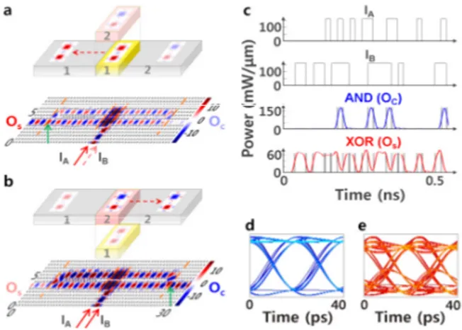
With the success in the ultra-low-power high-speed operation of photonic junction diode and all-optical regeneration using the simplest Ψe-o-ψo junction, we now consider another example for the modular application of mode junction. Half-adder, being the core building block for the Arithmetic Logic Unit (ALU) in the modern Central Processing Unit (CPU), has been often considered in the photonic domain [13,14], but mostly as the combination of discrete components, and also lacking isolation properties.
Fig. 5. Multi-junction realization of monolithic half-adder; (a) coupling to S (XOR) port with a single logic input (IA or IB) power below the threshold. (b) coupling to C (AND) port under two
input signals (IA · IB) for their total power above the threshold. Even (state 1)- / Odd (state 2)-
mode excitation for the central di-atomic resonator and couplings to the even- / odd- mode coupler at the S / C port (left / right) of the half-adder is evident from the FDTD generated field amplitude plot. Figure (c) shows the logic operations of AND & XOR, under the two input signals at 50Gbps (de-correlated, PRBS). Figure (d) and (e) show the optical eye patterns for AND & XOR outputs. To note, for the generation of phase / time synchronized two input signals (IA and IB) for the proper logic operation, a single source was assumed, which are power
For this, we stretch our design strategy one step further, to construct a monolithic, multi-junction half-adder (ψe-Ψe-o-ψo, shown in Fig. 5(a)); with the high-Q nonlinear region Ψe-o
sandwiched in-between ψe and ψo structures (in this case, even- and odd- mode couplers). Setting the input power of the logic signal (IA or IB) for Ψe-o resonator slightly below the
threshold of mode conversion, resonator even mode coupling only to the XOR output port (OS; supporting even mode) is enabled for a single input source (Fig. 5(a). 1← ψe-Ψe, Ψe-ψo → 0), meanwhile above the threshold with two input signals (IA · IB), the AND operation to the OC port (supporting odd mode) is activated with the nonlinear conversion to the odd mode in the center resonator (0 ← ψe-Ψo, Ψo-ψo → 1. Fig. 5(b)). Figure 5(c)–5(e) show the AND, XOR operation and their optical eye for the multi-junction monolithic half-adder, for the input of two PRBS NRZ signals at 50Gbps. Worth to note, under the arrangement of the multi-junction in three-level ψ2-Ψ(1/2/3)-ψ3 structure, for example with Tri-atom molecule states (T0,
T-, T + , in Fig. 1(b)), the same functionality with full input-to-output isolation could be achieved.
6. Conclusion
To summarize, we propose a mode junction for wave, with examples focusing on photonic applications. Rich and well-defined orthogonal modes providing ample degrees of freedom for the choice of junctions enable the modular construction of highly nonlinear devices of systematic control for wave propagation. By preferentially adjusting the optical potential, the dynamic and symmetry-breaking operation of the junction can be readily derived. For the simplest application of the formalism within a photonic crystal platform, we propose an ultra-low power photonic diode based on the Ψe-o-ψo junction, along with an application example for high speed signal regeneration. A superior performance in terms of orders has been realized when compared to previous results of photonic diode. Extending the concept further we then design a half-adder based on ψe-Ψe-o-ψo multi-junction, which provides all-optic AND and XOR output under a monolithic construction. The present examples operating in passive mode without external power, and providing highly nonlinear characteristics with an ultra-low threshold, we anticipate various applications beyond those demonstrated in this work.
Appendix
A. Details of the device structures and numerical method used in the study
Fig. 6. Layout of the photonic junction diode (case of Q = 1094). Red ellipsoids are dielectric defects composing di-atomic nonlinear resonators. Blue marked rods are position shifted (parameters in Table 1) in order; to introduce phase shift of π between the upper and lower waveguides (Box C, D), to fine-tune the resonance of the upper resonator (Box A), and to adjust couplings into the waveguide (Box B).
Table 1. List of Structural Parameters for the Photonic Junction Diode Layout in Fig. 6
Rods ∆x ∆y Purpose A 0.10a 0 Matching of ω1,2
B 0.05a 0 Matching of τR1,2
C 0 - 0.15a
Phase shift for odd mode coupler D 0 - 0.15a
Square-lattice, rod-type photonic crystal platform was considered for the design of photonic junction diode and monolithic multi-junction half-adder (To note, the use of square rod platform is for the design convenience [12,14,23,33]. For real implementations, it is necessary to consider the vertical confinement, for example by using a line-defect waveguide with small radius rods, or by adopting hole-type photonic crystal). The detailed schematics for junction diode, and parameters for the photonic crystal design are illustrated and summarized in Fig. 6 and Table 1. The radius of the dielectric rod was set to 0.2a (lattice constant a = 573nm), assuming the linear and nonlinear refractive index n and n2 to be 3.5 and 1.5x10
−17
m2/W respectively [34] (of AlGaAs. these values are within typical number range, when compared to other Kerr medium [1,2,4,35] or previous publications [12,14,25,26,33]). In the FDTD implementation, n2 equivalent nonlinear susceptibility value of χ(3) = 6.50x10⁻¹⁹m2/V2 [36] were used, following [31] to treat instantaneous Kerr nonlinear polarization term. The major and minor axis of the ellipsoidal rods comprising the di-atomic resonator were set to 0.64a and 0.54a in order to support two-band resonances at 193.24THz (1551.4nm, ψe) and 193.55THz (1548.9nm, ψo) with negligible spectral mode overlap (< e / o > = 0.16. Worth to note, this residual mode overlap determines the breakdown power under reverse bias (approximately, Pthreshold / Pbreakdown ~ <e/o>2 / <e/e>2). Considering both the device speed and power consumption, the loaded Q factor and modal volume V of the di-atomic resonator was set and measured to be 1094 and 0.19µm2 for the junction diode. To note, considering the experimental realization of 3D high-Q cavity (> 107 [37]), and the maximum loaded Q value (<105) assumed here, the criteria of Qintrinsic >> Qloaded is well met. For the design of the phase shifter in the ψe, or ψo coupler, the location of a few dielectric rods (Box C, D in Fig. 6) were shifted toward / outward (push / pull) from the side of the photonic crystal waveguides. Both frequency domain (COMSOL Multiphysics) and time domain analysis (FDTD) was carried out in excellent agreement with the result of CMT, confirming the operation / principle of the proposed devices. For FDTD calculation, time step of 47.7 attoseconds and mesh size of λeff /20 was used for total simulation time up to 2.54ns (5.31x10⁷ time step), to generate eye diagrams for diode and half adder operation. To remove the effect of reflection at the boundary, perfectly-matched layer (PML) boundary condition was applied for the simulation space of 1,320 x 480 grids (31.5 x 11.5 µm2).
B. Coupled mode theory for the di-atomic photonic junction diode
B.1. Analytical model and coupled mode equations
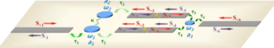
Fig. 7. Analytical model of the di-atomic mode junction diode, used in the temporal CMT analysis.
Temporal coupled mode theory was employed [12,33,38–40] to assess the behavior of the proposed junction diode. First, we write down the coupled mode equations for Fig. 7,
1 2 1 12 1 2 1 2 1 1 2 21 2 2 3 3 3 3 3 3 4 5 6 4 5 6 4 5 6 2 2 1 1 ( ) 0 1 2 0 1 1 1 2 2 2 0 0 ( ) S S i i a a d a i i a S dt a a i S S S ω κ τ τ τ τ κ ω τ τ ω τ τ τ τ τ τ + + + + + + + − − + = − − + − − + + + + (1) 1 1 1 1 2 2 2 2 2 S S a S S τ τ − + − + = − + (2) 3 3 2 3 2 S S a τ − = − + + (3) 4 4 4 5 5 3 5 6 6 6 2 2 2 S S S S a S S τ τ τ − + − + − + = − + (4) 1 2 4 4 2 j S S e S S θ + − + − = (5) 2 3 5 5 3 j S S e S S θ + − + − = (6)
B.2. Solution of resonator field (a1, a2, a3)
Solving Eqs. (2)–(4) and Eqs. (5) and (6) together we now arrive at the following expressions for the wave components entering to the resonators 1, 2, and 3.
1 2 4 2 1 3 21 1 23 3 1 1 2 2 2 sin 2 sin i e S a a a a i i θ τ τ α α θ θ + − = + ≡ + (7) 2 3 5 3 2 3 32 2 33 3 2 2 2 2 2 sin 2 sin i e S a a a a i i θ τ τ α α θ θ + − = + ≡ + (8) 1 2 4 4 1 3 41 1 43 3 1 1 2 2 2 sin 2 sin i e S a a a a i i θ τ τ α α θ θ + − = + ≡ + (9)
2 3 5 5 2 3 52 2 53 3 2 2 2 2 2 sin 2 sin i e S a a a a i i θ τ τ α α θ θ + − = + ≡ + (10)
Substituting Eqs. (7)–(10) into Eq. (1), the field amplitudes in resonators a1 ~a3 can be obtained to give, 6 2 2 2 5 1 12 6 3 1 3 6 1 6 2 6 21 21 2 2 2 1 5 4 12 3 3 3 3 2 2 ( ) ( ) ( )( ) ( )( ) c M c M c S c S c c a c M c c c c c M M c c c c c c c τ + τ + − − + − = − − − − − (11) 6 21 21 2 4 1 1 6 3 1 3 6 2 6 2 6 21 21 2 2 2 1 5 4 12 3 3 3 3 2 2 ( ) ( ) ( )( ) ( )( ) c c c c c S M S c c a c M c c c c c M M c c c c c c c τ + τ + − − + − = − − − − − (12) 6 2 2 2 5 1 12 6 3 1 3 6 4 2 21 5 3 6 2 6 21 21 2 2 2 3 5 6 2 1 5 4 12 3 3 3 3 2 2 ( ) ( ) ( )( ) ( )( ) c M c M c S c S c c c M c c a c M c c c c c M c c c M M c c c c c c c τ + τ + − − + − − = ⋅ − − − − − − (13) where 1 1 21 1 2 2 1 1 2 ( ) ( ) M i ω ω α τ τ τ = − − + + (14) 2 2 32 3 3 1 2 ( ) M i ω ω α τ τ = − − + (15)
and cij’s are constant values not affected by the nonlinear frequency shift ; c12 = iκ12, c21 = iκ21,
c2 = (2/τ2) 1/2 α23, c3 = (2/τ3) 1/2 α33, c4 = (2/τ4) 1/2 α41, c5 = (2/τ5) 1/2 α52, and c6 = i(ω–ω3) – (1/τ4 + 1/τ5 + 1/τ6) + (2/τ4)1/2α43 + (2/τ5)1/2α53.
B.3. Implementation of Kerr nonlinearity and Calculation of Diode Throughput
It is important to note that, in order to calculate the field energy in the resonators (|a1|
2
and |a2|2) from Eq. (11) and (13), we also incorporate the resonance-red-shift from the Kerr nonlinearity for the resonator 1 and 2, using ωk = ωk
0 –ρ|ak| 2 (k = 1, 2), where ωk 0 is the resonance frequency without nonlinearity, and ρ is σωk0(n2/n0)·(c/n0Vkerr), σ being the fraction of the mode energy stored in the nonlinear modulated region, c is the light speed, Vkerr is the modal volume of the nonlinear resonator and n2 is the nonlinear Kerr coefficient.
The transmitted optical power for the forward and reverse bias condition can then be calculated from Eq. (11) and (13), by using a simple relation, PO = (2 / τ6)|a3|2 for forward feeding boundary condition |S+1|2 = PI, S+6 = 0, and PO = (2 / τ1)|a1|2 for the reverse feeding boundary condition |S+6|2 = PI, S+1 = 0. Specifically, applying boundary conditions for forward bias, the expression for the stored field energy |a3|
2 of resonator 3 becomes 2 2 1 5 4 2 2 3 2 1 3 5 6 2 c c c M a a c c c M − = − (16)
where for Eq. (16), M1(|a1|
2
) and M2(|a2|
2
) can be calculated from Eqs. (14), (15) with resonance shifted frequency ωk = ωk0–ρ|ak|2 and for |a1|2 and |a2|2 being
2 6 2 5 2 3 1 1 2 6 2 6 21 21 2 2 2 1 5 4 12 3 3 3 3 2 ( )( ) ( )( ) I c M c P c a c M c c c c c M M c c c c c c c τ − = − − − − − (17) 2 2 2 3 4 6 21 2 2 1 3 5 6 2 . a c c c c a c c c M − = − (18)
For reverse bias boundary condition, the stored field energy |a1|2 can be reduced to give,
2 2 2 12 2 3 6 1 2 6 2 6 21 21 2 2 2 1 5 4 12 3 3 3 3 2 ( )( ) ( )( ) I c M c P c a c M c c c c c M M c c c c c c c τ − = − − − − − (19)
where M1(|a1|2) and M2(|a2|2) can be calculated from, by setting ωk = ωk0–ρ|ak|2 and using,
2 2 2 3 1 2 21 2 2 1 3 12 2 2 . a c M c c a c c c M − = − (20)
The output power thus then can be obtained from PO = (2 / τ6)|a3|2 for forward feeding, or with PO = (2 / τ1)|a1|
2
for reverse feeding. Using the FDTD measured resonator parameter sets
ωk0, ρ, τi, and θi , the transmission power and response curve of the diode (Fig. 4(a)) can be finally obtained using equation for PO separately for forward bias and reverse bias.
Acknowledgment
We acknowledge helpful discussions with Prof. Kwang Seok Seo, regarding the history / significance of junction structures in electronics. This work was supported by the National Research Foundation (GRL, K20815000003 and SRC 2011-0001054) funded by the Korean government.