https://doi.org/10.6113/JPE.2019.19.6.1380 ISSN(Print): 1598-2092 / ISSN(Online): 2093-4718
JPE 19-6-4
Research on Grid Side Power Factor of Unity
Compensation Method for Matrix Converters
Yihui Xia
*, Xiaofeng Zhang
*, Zhihao Ye
†, and Mingzhong Qiao
*†,*Department of Electric Engineering, Naval University of Engineering, Wuhan, China
Abstract
Input filters are very important to matrix converters (MCs). They are used to improve grid side current waveform quality and to reduce the input voltage distortion supplied to the grid side. Due to the effects of the input filter and the output power, the grid side power factor (PF) is not at unity when the input power factor angle is zero. In this paper, the displacement angle between the grid side phase current and the phase voltage affected by the input filter parameters and output power is analyzed. Based on this, a new grid side PF unity compensation method implemented in the indirect space vector pulse width modulation (ISVPWM) method is presented, which has a larger compensation angle than the traditional compensation method, showing a higher grid side PF at unity in a wide output power range. Simulation and experimental results verify that the analysis of the displacement angle between the grid side phase current and the phase voltage affected by the input filter and output power is right and that the proposed compensation method has a better grid side PF at unity.
Key words: Grid side power factor (PF), Indirect space vector pulse width modulation (ISVPWM), Input filter, Matrix converter
(MC), Output power
I. I
NTRODUCTIONThe matrix converter (MC), as an AC-AC power electronic converter device, can fulfill all of the requirements of the traditionally used AC/DC/AC structures of power converters. In addition, it can provide efficient ways to convert electric power for motor drives, and has the following advantages [1]-[3].
(1) High power density, with no bulky DC link component. (2) Sinusoidal input and output current.
(3) Adjustable input power factor. (4) Regeneration capability.
The input filter in an important component of MCs, It is used to improve the grid side current quality with low harmonic components. It is also able to reduce the input voltage distortion supplied to the grid side. Therefore, there are many studies devoted to input filter designs [4]-[10]. In [4], an automated design procedure to select and optimize
both the topology and the parameters of the input filter for an MC based on a genetic algorithm (GA) was proposed. The GA optimize structure and the parameters of the input filter as a function of different factors can be applied to many converter configurations. In [5] and [6], input filter designs for sliding mode controlled MCs consider the maximum allowable displacement angle introduced by the input filter and the controllable grid side PF capability, as well as the ripple of input voltages. The integration of an MC with filters is presented in [7], which provides a lower electromagnetic interference, lower common-mode current and lower shaft voltage. Input filter optimization for a DTC driven matrix converter-fed PMSM drive is analyzed and the optimization is performed using the Cuckoo Search method in [8]. Cuckoo Search has better quality indicators of the input filter than the analytical method. Aiming at the resonances in the input filter of an MC with the classic model predictive control, two methods have been proposed to mitigate the resonances in the input filter in [9]. Both of the methods can significantly reduction the harmonic distortion produced by the input filter.
However, if the input filter is not well designed in conjunction with the control system of the MC, it can generate an instability problem of the whole system [11]-[16]. Several papers have discussed the stability of an MC affected © 2019 KIPE
Manuscript receivedDec. 29, 2018; accepted Jun 21, 2019 Recommended for publication by Associate EditorHuiqing Wen. †Corresponding Author: yxyx928@126.com
*Dept. of College of Electric Engineering, Naval University of Engineering, China
by input filter parameters. In [11], a small-signal analysis around a steady-state operating point was introduced to analyze the stability of an MC. It paid more attention to the delay time introduced in the digital controllers. In addition, the system may be unstable since the output power exceeds a limit value. The analyses in [12] and [13] show that the power limit can be increased if the duty cycles of the switching configurations are calculated using filtered input voltages. Although the capability of the MC to compensate input voltage disturbances is affected to some extent, the stability limit can be sensibly improved with a digital low- pass filter. In [15], the stability of an MC is analyzed by considering the change of the input impendence with the input current control, which can be used to select control parameters. A general constructive approach to matrix converters is analyzed in [16], and the stability of the MC is improved by constructing a correction term to increase the input impendence of the MC.
In addition, the stability of the MC is affected by the input filter. This also results in a displacement angle between the grid side phase current and phase voltage when the input PF angle is set to 0. In the case of low output power/voltage transfer ratio conditions, the grid side PF decreases significantly. To achieve a grid side PF at unity control, several papers have proposed compensation methods [17]-[22]. In [17], a closed-loop input displacement factor correction is used to adjust the grid side current phase shift according to the load level. In [18], a model predictive control is used and a cost function is built based on the output current error, common- mode voltage, and minimum reactive power in the grid side. Since 27 switch states are calculated in a switch period, the computational amount is very large. Two grid side PF compensation algorithms were proposed in [19]. One is based on a mathematical model for the grid side of the MC, and the other is based on closed-loop control with a PI controller. The method based on a mathematical model for the grid side of the MC has good steady performance of the grid side PF at unity control under a high output power. However, the performance of the grid side PF at unity control with a low output power is not satisfied. In [20], a novel unity power factor fuzzy battery charger using an ultra-sparse matrix converter was proposed. Its advantages are a low harmonic distortion and a near unity power factor over a wide operating output power range. A current control with instantaneous reactive power minimization for an indirect MC was proposed in [21]. The best-suited switch state considering the output voltage error and the input power factor is evaluated by predicting the values of the input and output current in the control scheme. In essence, it is still a model predictive control method that needs a large number of calculations. A hybrid indirect modulation strategy based on extending the reactive input power operating range of an MC was proposed in [23]. It can be generalized to an arbitrary load condition by
using the pulse merging and compensation principal, which leads to an increased reactive power control range. However, the hybrid modulation strategy needs to use appropriate schemes such as two-vector, three-vector and optimum schemes, which adds to the complexity of the modulation strategy. A novel modulation method based on the mathematical construction method for an MC is proposed in [24], which can enhance the control range of the input reactive power with low computational efforts. The maximum input reactive power with the method proposed in [24] is higher than that with the optimum-amplitude method and the indirect SVM method. Two modulation methods for an indirect MC were proposed to extend the input reactive power in [25]. First, they are divided into two independent parts: the output voltage formation and input reactive current formation. In terms of the input reactive power range, they are superior to the traditional indirect SVPWM in most situations.
In addition, an MC has been successfully employed in a DFIG-based VSCF WECS in different operation modes, and its input reactive and active power have been researched in [26]-[31]. In [26], the maximum active and reactive power capability of a matrix converter-fed DFIG-based wind energy conversion system is analyzed, and the maximum possible reactive power support by the MC under different operating conditions is accurately predicted by using a new steady-state model of the MC. In [15], a new source current control strategy that can improve both the source current quality and the input factor was proposed for an indirect MC with an asymmetric mode. However, the control strategy needs a large number of calculations and is complex. In [27]-[29], several control techniques such as direct power control, vector control and direct torque control are used in DFIG-based VSCF WECS. In [30], a singular value decomposition-based modulation strategy for an MC supplying a permanent magnet synchronous wind generator was proposed, which can significantly improve the input reactive power supply capability of the MC.
To obtain a higher performance of the grid side PF with the unity control method, the effect on the grid side PF is analyzed by building a mathematical model of the MC in this paper. Based on this, a new grid side PF at unity control method is presented by analyzing the grid side reactive power. In addition, the compensation angles with the proposed and traditional compensation methods are compared, and the compensation angle with the proposed method is shown to be larger than that with the traditional compensation method, showing a better grid side PF at unity. Simulation and experimental results verify that theoretical analysis is right and that the proposed method is feasible.
This paper is organized as follows. In section II, the basic structure of a direct MC is introduced and the displacement angle between the grid side phase current and phase voltage affected by the input filter and output power is analyzed. In
section III, a new grid side PF with a unity compensation algorithm is proposed based on the analysis in section II, and the compensation angles of the proposed and traditional compensation methods are compared. In section IV, simulations are carried out with the traditional ISVPWM method, the compensation method in [19], and the proposed compensation method in this paper. In section V, experiments are carried out to verify the validity of the analysis of the displacement angle affected by the input filter and output power, and the effectiveness of the proposed compensation method in the paper. Finally, some conclusion are presented in Section VI.
II. D
ISPLACEMENTA
FFECTED BY THEI
NPUTF
ILTER ANDO
UTPUTP
OWERA. Basic Structure of a Direct Three-phase to Three-phase MC
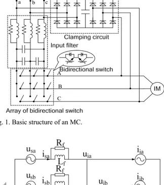
Fig. 1 shows the basic topology structure of a three-phase to three-phase direct MC, which is composed of an input filter, a bidirectional flow switch and a clamping circuit. The input filter is used to improve the grid side current quality with low harmonic components, and to reduce the input voltage distortion supplied to the grid side. The clamping circuit is designed for over-voltage protection, and the bidirectional switch is used to synthesize a desired output voltage and input current.
B. Grid Side Mathematical Model of an MC in the Synchronous Reference Frame
From Fig. 1, a three-phase input equivalent circuit can be shown as in Fig. 2. In this figure, the output side is seen as a current source.
From Fig. 2, the grid side mathematical model in the a-b-c coordinates can be obtained as:
(1)
(2)
Where . The grid side
rotates with the input angular frequency ωi. In addition, (1)
and (2) can be expressed in the synchronous reference frame
Fig. 1. Basic structure of an MC.
Fig. 2. Three-phase equivalent circuit of an MC.
as (3) and (4), respectively.
(3)
(4)
The steady state operation points, such as isd and isq, of the
whole system can be obtained by letting the derivation of isd, isq, Uid and Uiq be set to 0.
(5)
The grid side voltage Usj(j=a,b,c) and the input current iij
are obtained as follows:
(6) ic sc sc sc ib sb sb sb ia sa sa sa U U Ri dt di L U U Ri dt di L U U Ri dt di L ic sc ic f ib sb ib f ia sa ia f i i dt dU C i i dt dU C i i dt dU C 2 2 2 2 2 2 2 2 2 f i f f i f f i f f f L R L R R , L R L R L a b c A B C iq sq sd i sq sq id sd sq i sd sd U U i Ri dt di L U U i Ri dt di L
iq id i sq iq f id iq i sd id f i U i dt dU C i U i dt dU C
2 2 2 2 2 2 2 2 2 2 1 1 1 1 R C LC Ri C i U C LC i R C LC Ri C RU C i LC i f i f i id f i iq sd f i f i sq f i f i iq f i sd f i id f i sd
3 2 3 2
t cos U U t cos U U t cos U U i im sb i im sb i im sa(7)
Where Uim is the grid side phase voltage amplitude, Iim is
the grid side phase voltage amplitude, and φi is the input
phase current amplitude and input power factor angle. From (6) and (7), Usd, Usq, iid and iiq can be expressed as follows:
(8)
Substituting (8) into (5), isd and isq can be rewritten as
follows:
(9)
The grid side active power p and reactive power q can be calculated as follows:
(10) When the input P is set to 0, that is to say, cosφi=1,sinφi=0,
(10) can be simplified as follows:
(11)
From (11), it can be known that the reactive power q has something to do with the input filter parameters and the input current amplitude Iim. To conveniently analyze how p and q
are affected by the input filter parameters and the input current amplitude, the parameters of the input filter and the input current amplitude are shown in Table I.
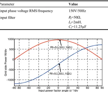
C. Grid Side PF affected by the Damping Resistor Rf
Fig. 3 shows the relationship between the grid side power and the input power factor angle φi under different damping
resistors. The solid line is the active power p and the dotted line is the reactive power q. The grid side active power p and reactive power q have not been greatly changed with Rf
increased in the condition where φi is a constant. In particular,
when φi is set to 0°, p and q are near 956W and -239W,
respectively. In this condition, the displacement angle is 14°and the grid side PF is 0.97. When φi decreases from 0° to
-90°, p is decreased and q is increased, resulting in a decrease in the grid side PF. When φi increases from 0° to14°, both p
TABLE I
PARAMETERS OF THE INPUT FILTER AND THE INPUT CURRENT
AMPLITUDE
Parameter Value
Input phase voltage RMS/frequency 150V/50Hz
Input filter Rf=50Ω,
Lf=2mH, Cf=11.25µF
Fig. 3. Variations of the grid side active power and reactive power with input power factor angle φiunder different damping
resistors.
Fig. 4. Variations of the grid side power with the input power factor angle φi under different filter inductances.
and q are decreased. However, q is decreased faster than p. When φi increases from 14° to 90°, p is decreased and q is
increased, resulting in a decrease of the grid side. It should be specially noted that when φi is set to 14°, p is 0 and the grid
side PF is achieved at unity. The input PF angle φi is called
the compensation angle in the following sections of the paper.
D. Grid Side PF affected by the Filter Inductance Lf
Fig. 4 shows the relationship between the grid side power and the input power factor angle φi under different filter
inductances. The solid red line is active power p and the dotted blue line is the reactive power q. The grid side active power and reactive power are not greatly changed with an increase of Lf since φi is a constant. When φi is set to 0°, the
active power p and the reactive power q are near 956W and 239W, respectively. The displacement angle is still 14° and the grid side PF is 0.97. The grid side PF varies with φi. This
isalmost the same as what was just described in part C of
3 2 3 2
i i im ic i i im ib i i im ia t cos I i t cos I i t cos I i i im iq i im id sq im sd sin I i cos I i U U U 0
2 2 2 2 2 2 2 2 2 2 1 1 1 1 R C LC cos RI C sin I U C LC i R C LC sin RI C RU C cos I LC i f i f i i im f i i im im f i f i sq f i f i i im f i im f i i im f i sd
im f i f i i im f i i im im f i f i sq sd sd sq im f i f i i im f i im f i i im f i sq sq sd sd U R C LC cos RI C sin I U C LC i U i U q U R C LC sin RI C RU C cos I LC i U i U p 2 2 2 2 2 2 2 2 2 2 1 2 1 3 2 3 1 2 1 3 2 3
im f i f i im f i im f i f i sq sd sd sq im f i f i im f i im f i sq sq sd sd U R C LC RI C U C LC i U i U q U R C LC RU C I LC i U i U p 2 2 2 2 2 2 2 2 2 2 1 2 1 3 2 3 1 2 1 3 2 3 -90 -80 -60 -40 -20 0 20 40 60 80 90 -1000 -500 0 500 1000 IIIIIIIIIIIIIIIIIIIIIIIII IIIIIIIφ G III Is II II P II II IW II II RIR5 R50 R100Ω Ω Ω RIR5 R50 R100Ω Ω Ω -90 -80 -60 -40 -20 0 20 40 60 80 90 -1000 -500 0 500 1000 IIIIIIIIIIIIIIIIIIIIIIIII IIIIIIIφ G IIII sI III III III W IIII LIR1mHR2mHR4mH LIR1mHR2mHR4mHFig. 5. Variations of the grid side power with the input power factor angle φi under different filter capacities.
Fig. 6. Variations of the grid side power with the input power factor angle φi under different input current amplitudes.
Section II when Rf is a constant.
E. Grid Power Affected by the Filtered Capacity Cf
Fig. 5 shows the relationship between the grid side power and the input power factor angle φi under different filter
capacities. The solid line is the active power p and the dotted line is the reactive power q. It can be seen that the grid side active power p is largely unchanged. However, the reactive power q is greatly changed with an increase of Cf when φi is a
constant. When φi is set to 0°, the active power p is near
956W, and the reactive powers q are -106.2W (5µF), -239W (11.25µF) and -425.6W (20µF). The corresponding displacement angles between the grid side phase voltage and the phase current are 6.4°, 14° and 24°, and the grid side PFs are 0.99, 0.97 and 0.914, respectively. The grid side PF varies with φi almost the same (only the compensation angle is
changed) as that described in part C of Section II when Cf is a
constant.
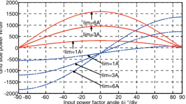
F. Grid Power Affected by Input Current Amplitude Iim
Fig. 6 shows the relationship between the grid side power and the input power factor angle φi under different input
current amplitudes (since the input power is equivalent to the load power, when Iim varies, it can be seen that the load
power varies). The solid red line is the active power p and the dotted blue line is the reactive power q. As can be seen, both the grid side active power p and the reactive power q (except for φi=0°) is largely changed when Iim is increased when φi is
a constant. When φi=0°, the active power p is largely changed
(1A, 319.2W; 3A, 956W; 6A, 1594.4W) and the reactive power does not change and is still 239W. The corresponding displacement angles between the grid side phase voltage and the phase current are 36.8°, 14° and 8.6°, and the grid side PFs are 0.8, 0.97 and 0.989, respectively. The grid side PF varies with φi which is almost the same (only the
compensation angle is changed) as that described in part C of Section II when Iim is a constant. In addition, q changes faster
when Iim is increased and the grid side PF is not at unity
control.
III. P
ROPOSEDG
RIDS
IDEPF
W
ITH THEU
NITYC
OMPENSATIONM
ETHODI
MPLEMENTEDIN THE
I
NDIRECTSVPWM
A. Proposed Grid Side Power with the Unity Compensation Method
According to (10), to achieve the grid side PF at unity control, the grid side reactive power q must be set to 0, which can be expressed as (12).
(12)
To obtain the compensation angle φi,(12) is rewritten as
follows:
(13) Since the input active power is equal to the output active power, the following equation exists:
(14)
Where Uom, Iom and φL are the output phase voltage
amplitude, the output phase current amplitude, and the load power factor angle. In (14), a grid side voltage approximately equal to the filter capacity voltage uij is used. Substituting (14)
into (13), φi is derived as follows:
(15)
In (15), R is so small that it can be ignored, and (15) can be rewritten as (16).
(16)
Substituting (14) into (16), (16) can be rewritten as (17).
(17)
From (12), it can be known that as long as φi is set as in
-90 -80 -60 -40 -20 0 20 40 60 80 90 -1500 -1000 -500 0 500 1000 IIIIIIIIIIIIIIIIIIIIIIIII IIIIIIIφ G III Is IIII III II IW II II CIR5IF CIR11.25IF CIR20IF CIR5IFR11.25IFR20IF -90 -80 -60 -40 -20 0 20 40 60 80 90 -2000 -1500 -1000 -500 0 500 1000 1500 2000 IIIIIIIIIIIIIIIIIIIIIIIII IIIIIIIφ G III Is II II II I II IW II II IImR1A IImR1A IImR3A IImR6A IImR6A IImR3A
1 2
0 i im f i i im im f i f iLC C U I sin C RI cos
i i f i i im im f tan L C R cos I U LC i 1 1 2 L om om i im imI cos U I cos U
1 2
2 57.3 tan 1 om om L i f im i om om L i i f RU I cos LC U a U I cos L C 2 57.3 tan cos i f im i om om L C U a U I 57.3 i f im i im C U asin I Fig. 7. Compensation angles varying with Iim with the proposed
and traditional compensation methods.
(17), a grid side PF at unity can be achieved. Therefore, the proposed grid side PF at unity compensation method is obtained, and it is an online method by measuring and calculating the amplitude of the input voltage and input current. From (17), it is known that the proposed grid side PF at unity compensation method is obviously affected by the output power and filter capacitor. However, it is almost independent of the input filter inductance and damped resistance. This is consistent with section II.
B. Comparative Analysis of the Proposed and Traditional Compensation Methods
In [19], the traditional compensation angle φi is calculated
as follows:
(18) The compensation angles with the proposed method and the traditional method varying with the input current amplitude
Iim are shown as Fig. 7. The input filter and input voltage
parameters are set as in Table. I. It can be seen that the compensation angle with the proposed method is larger than that with the traditional method. This shows that the proposed compensation method has a better grid side PF at unity than the traditional compensation method.
The duty ratio of the zero switch has to be positive to validate the grid side power factor under unity control in [19]. At the same time, the method in [19] is only validated if the input current vector leads the input voltage vector to one sector, i.e., φimax ≤ 60°. In addition, the maximum
compensation angle φimax is defined as follows:
(19) However, when VTR ≤ , the duty ratio of the zero
switch is positive in most cases. In (26), if d0<0 or d0=0, the
duty ratios d1, d2, d3 and d4 are modified as follows:
(20)
Fig. 8. Fictitious AC-DC-AC structure of a matrix converter.
Taking into account both the input power factor and the systematic stability, the maximum compensation angle φimax
is restricted as 80° from Fig. 7. In addition, its corresponding
VTR =0.14. Therefore, under the condition of a low VTR, the
maximum compensation angle can be appropriately enlarged to further improve grid side PF on the premise of ensuring system stability. The enlarged φimax as follows:
(21)
C. Proposed Compensation Method Implemented in the Indirect SVPWM of an MC
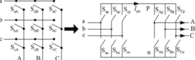
An MC can be considered as a fictitious AC-DC-AC structure, which is shown in the right half plane of Fig. 8. The AC-DC can be seen as a voltage source rectifier (VSR) in the input side and the DC-AC can be seen as a voltage source inverter (VSI) in the output side. Both the VSR and the VSI use SVPWM. Then the relation between the MC structure and the fictitious AC-DC-AC structure is utilized to obtain the duty ratio of each switch in the MC.
The combination of two switches in the VSR and two switches in the VSI results in four switches in the MC. The final duty ratio of the four active and one zero switching configurations with the traditional SVPWM can be obtained as follows:
(22)
Where the voltage transfer ratio VTR=Uom/Uim, and θj and θi
are the output voltage vector and the input current vector angles, respectively. From section II, it can be known that the grid side phase current usually leads the phase voltage due to the input filter and the output power. That is to say, when the input PF angle δ=0, the grid side PF is not at unity. To achieve the grid side PF at unity control, the input current vector phase angle must be modified to eliminate the effect of
0 0.5 1 1.5 2 2.5 3 3.5 4 4.5 5 10 20 30 40 50 60 70 80 90 100 IIIIIIIIIIIIIIImIIIIIIIIIImIIAIIII D II II IIII I ThIIIIIIIIIIIIIImIIhII ThIIIIIIIsIIImIIhII
2
57.3 tan 1-i f im i i f f im C U a L C I
imax 57.3 cos 2 3 , 3 4 3 2 0 3 4 60, TR TR TR a V V V 2 3 4 3 2 1 4 3 2 1 , , , i, d d d d d d i i
imax 57.3 cos 2 3 ,0.14 3 2 0 0.14 80, TR TR TR a V V V
1 i 2 i 3 i 4 i 0 1 2 3 4 2 sin sin 3 2 3 cos 2 sin sin 3 6 3 cos 2 sin sin 2 3 cos 2 sin sin 6 3 cos 1 TR m j i TR n j i TR m j i TR n j i V d d d V d d d V d d d V d d d d d d d d TABLE II SIMULATION PARAMETERS
Parameters Values Input phase voltage RMS/frequency 150V/50Hz
Input filter Rf=50Ω, Lf=2mH, Cf=11.25µF Switch frequency 5kHz R-L Load R=25Ω, L=8mH
the low-pass input filter. As long as the grid side reactive power q=0, the grid side PF must be at unity, and (22) is modified as (23).
(23)
Where (23) θi=θv-φi, θv is the input voltage vector angle.
IV. S
IMULATIONR
ESULTS ANDD
ISCUSSIONS A simulation model of a direct three-phase to three-phase MC is built with MATLAB/Simulink software. The load is the R-L type. The simulation parameters are listed in Table II.A. Grid Side PF Affected by the Input Filter and the Output Power
Fig. 9(a) through Fig. 9(d) show simulation results of the traditional SVPWM method at a referenced output voltage of
VTR=0.44, and an output frequency of fo=10Hz under different
input filter parameters and output powers.
From Fig. 9(a) and Fig. 9(b) it can be seen that the grid side phase current isa leads the grid side phase voltage usa, the
active power is 495W, and the reactive power is -250W regardless of whether Rf is 50Ω or 100Ω. The grid side PF is
0.892. Simulation results indicate that the damping resistor has small impact on the grid side PF.
Fig. 9(c) shows simulation results of the MC with the filter inductance changed to 4mH. When comparing Fig. 9(a) to Fig. 11(c), it can be seen that isa still leads usa, the active
power is 510W, and the reactive power is -250W when Lf is
4mH. The grid side PF is a slightly improved to 0.897. However, it is not greatly changed, which indicates that the filter inductance Lf has a small impact on the grid side PF.
Fig. 9(d) shows simulation results of the MC with the filter capacity Cf increased to 20µF. When comparing Fig. 11(a) to
(a)
(b)
(c)
(d)
Fig. 9. Input/output waveforms with the traditional SVPWM method at VTR=0.44 fo=15Hz for: (a) Rf=50Ω, Lf=2mH,
Cf=11.25µF(PF=0.892), (b) Rf=100Ω, Lf=2mH,
Cf=11.25µF(PF=0.892), (c) Rf=50Ω, Lf=4mH,
Cf=11.25µF(PF=0.897), (d) Rf=50Ω, Lf=2mH,
Cf=20µF(PF=0.762).
Fig. 9(d), isa leading usa is increased, the active power is
500W, and the reactive power is -425W. The grid side PF is decreased from 0.892(11.25µF) to 0.762(20µF), which indicates that grid side PF is decreased with an increase of the filter capacity Cf.
4 3 2 1 0 4 3 2 1 1 6 3 2 2 3 2 6 3 3 2 2 3 3 2 d d d d d sin sin cos V d d d sin sin cos V d d d sin sin cos V d d d sin sin cos V d d d i j i TR n i j i TR m i j i TR n i j i TR m 0 0.01 0.02 0.03 0.04 0.05 -400 0 400 0 0.01 0.02 0.03 0.04 0.05 -2 0 2 0 0.01 0.02 0.03 0.04 0.05 -3000 500 0 0.01 0.02 0.03 0.04 0.05 -400 0 400 0 0.01 0.02 0.03 0.04 0.05 -5 0 5 IIs q IsIIAIIII UABIVIIII IAIAIIII PIIIIIWIIII I UsIIVIIII 0 0.01 0.02 0.03 0.04 0.05 -400 0 400 0 0.01 0.02 0.03 0.04 0.05 -2 0 2 0 0.01 0.02 0.03 0.04 0.05 -3000 500 0 0.01 0.02 0.03 0.04 -400 0 400 0 0.01 0.02 0.03 0.04 0.05 -5 0 5 IIs q IsIIAIIII UsIIVIIII UABIVIIII IAIAIIII PIIIIIWIIII I 0 0.01 0.02 0.03 0.04 0.05 -400 0 400 0 0.01 0.02 0.03 0.04 0.05 -2 0 2 0 0.01 0.02 0.03 0.04 0.05 -3000 500 0 0.01 0.02 0.03 0.04 0.05 -400 0 400 0 0.01 0.02 0.03 0.04 0.05 -5 0 5 IIs q IsIIAIIII UABIVIIII I UsIIVIIII PIIIIIWIIII IAIAIIII 0 0.01 0.02 0.03 0.04 0.05 -400 0 400 0 0.01 0.02 0.03 0.04 0.05 -5 0 5 0 0.01 0.02 0.03 0.04 0.05 -5000 500 0 0.01 0.02 0.03 0.04 0.05 -400 0 400 0 0.01 0.02 0.03 0.04 0.05 -5 0 5 IIs q IsIIAIIII UABIVIIII I UsIIVIIII IAIAIIII PIIIIIWIIIIFig. 10. Input/output waveforms with the traditional SVPWM at
VTR=0.58 fo=20Hz for Rf=50Ω, Lf=2mH, Cf=11.25µF(PF=0.95).
The waveforms shown in Fig. 10 are simulation results of an MC with the traditional SVPWM method at a referenced output voltage of VTR=0.58, fo=20Hz. The grid side phase
current leading phase voltage is reduced when compared to Fig. 9(a). The active power is increased to 885W, the reactive power is -270W, and the grid power PF is improved to 0.95. It can be known that the grid power PF is increased when the output power is increased and that the reactive power is not greatly changed.
B. Proposed Grid Side Power Factor under Unity Control
Fig. 11 shows dynamic performances of VTR changing from
VTR=044, fo=15Hz to VTR=0.58, fo=20Hz with the traditional
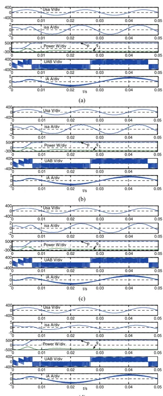
SVPWM method, the traditional compensation method, and the proposed compensation method, respectively. The displayed waveforms show that the grid side phase current is controlled to be in phase with the grid side phase voltage with the two compensation methods in [19] and the proposed method in this paper. When VTR=0.44, fo=15Hz, the grid side
PF is 0.99(p=510W, q=70W) with the compensation method in [19]. The grid side PF is 0.997(p=510W, q=35W) with the proposed compensation method. When VTR=0.58, fo=20Hz,
the grid side PF is 0.995(p=910W, q=90W) with the traditional compensation method. The grid side PF is 0.998(p=910W, q=55W) with the proposed compensation method in this paper. Both of the compensation methods have improved the grid side PF from 0.892(VTR=0.44, fo=15Hz)
and 0.95(VTR=0.58, fo=20Hz) to the unity. In addition, it can
be seen that the proposed method has higher grid side PF by comparing the two compensation methods.
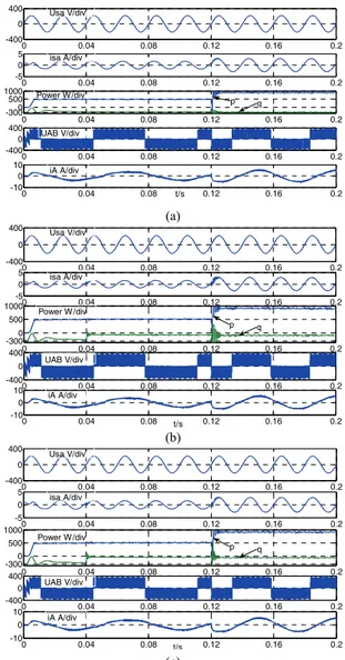
Fig. 12(a) through Fig. 12(c) show steady-state performances at VTR=0.22, fo=7.5Hz of the traditional SVPWM, the
traditional compensation method, and the proposed compensation method, respectively. As can be easily seen, the grid side phase current is almost in phase with the phase voltage in Fig. 12(c), and the grid side phase current leads the phase voltage in Fig. 12(a) and Fig. 12(b). In particular, it is exceedingly obvious in Fig. 12(a). The grid side phase currents and phase voltage waveforms in Fig. 11(a) represent the grid side PF at 0.447(p=120W, q=240W), and in Fig. 12(b) they represent the grid side PF at 0.8(p=135W, q=100W). The
(a)
(b)
(c)
Fig. 11. Input/output waveforms of an MC as VTR changes from
VTR=0.44, fo=15Hz to VTR=0.58, fo=20Hz for the: (a) Traditional
SVPWM method, (b) Traditional compensation method, (c) Proposed compensation method.
grid side phase currents and phase voltage waveforms in Fig. 9(c) represent the grid side PF at 0.989(p=135W, q=20W). Although both of the compensation methods have the ability to improve the grid side PF, the proposed compensation method shows better performances in terms of improving the grid side PF.
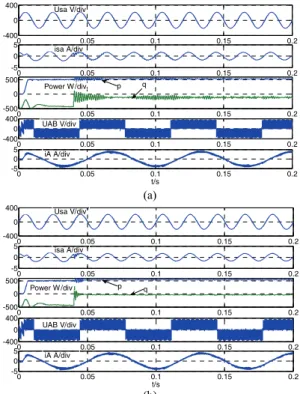
Fig. 13(a) and Fig. 13(b) show the steady-state and dynamic- state performances at VTR=0.44, fo=15Hz as well as the filter
capacity Cf 20µF of both the traditional compensation method
and the proposed compensation method, respectively. As can be seen, the grid side active power and reactive power in the steady-state vary immensely, and the grid side power oscillation in the dynamic-state process lasts a long time with the traditional compensation method. The grid side power oscillation in the dynamic-state process is very short, and the active power and reactive power in the steady-state vary slightly. In the steady-state, the grid side PF is 0.975(p is near
0 0.01 0.02 0.03 0.04 0.05 -400 0 400 0 0.005 0.01 0.015 0.02 0.025 0.03 0.035 0.04 0.045 0.05 -5 0 5 0 0.01 0.02 0.03 0.04 0.05 -3000 1000 0 0.01 0.02 0.03 0.04 0.05 -400 0 400 0 0.01 0.02 0.03 0.04 0.05 -10 0 10 IIs q IsIIAIIII UABIVIIII I UsIIVIIII IAIAIIII PIIIIIWIIII 0 0.04 0.08 0.12 0.16 0.2 -400 0 400 0 0.04 0.08 0.12 0.16 0.2 -5 0 5 0 0.04 0.08 0.12 0.16 0.2 -3000 500 1000 0 0.04 0.08 0.12 0.16 0.2 -400 0 400 0 0.04 0.08 0.12 0.16 0.2 -10 0 10 IIs PIIIIIWIIII UABIVIIII IsIIAIIII UsIIVIIII I q IAIAIIII 0 0.04 0.08 0.12 0.16 0.2 -400 0 400 0 0.04 0.08 0.12 0.16 0.2 -5 0 5 0 0.04 0.08 0.12 0.16 0.2 -3000 500 1000 0 0.04 0.08 0.12 0.16 0.2 -400 0 400 0 0.04 0.08 0.12 0.16 0.2 -10 0 10 IIs UsIIVIIII q I IAIAIIII PIIIIIWIIII UABIVIIII IsIIAIIII 0 0.04 0.08 0.12 0.16 0.2 -5 0 50 0.04 0.08 0.12 0.16 0.2 -400 0 400 0 0.04 0.08 0.12 0.16 0.2 -3000 500 1000 0 0.04 0.08 0.12 0.16 0.2 -400 0 400 0 0.04 0.08 0.12 0.16 0.2 -10 0 10 IIs UsIIVIIII PIIIIIWIIII q I IsIIAIIII UABIVIIII IAIAIIII
(a)
(b)
(c)
Fig. 12. Input/output waveforms of an MC at VTR=0.22, fo=7.5Hz
for the: (a) Traditional SVPWM method, (b) Traditional compensation method, (c) Proposed compensation method in this paper.
530W, q is near 120W) with the traditional compensation method, and grid side PF is 0.998 (p is near 540W and q is near 30W). The proposed compensation method still shows better performances in terms of the grid side PF under unity control with the filter capacity increased.
Fig. 14 shows comparisons of the grid side PF obtained from the traditional SVPWM method, the traditional compensation method, and the proposed compensation method, respectively. With a constant U/f 220V/50Hz for the R-L load, a higher output load corresponds to a higher VT R.
Compensation angles at the steady state; obtained from the traditional SVPWM method, the traditional compensation method, and the proposed compensation method; and the maximum compensation angle; obtained from the traditional compensation method and the proposed compensation method; are shown in Fig. 14(b). As can be easily seen from Fig. 14(a), with the high output voltage region VTR≥0.44, the
(a)
(b)
Fig. 13. Input/output waveforms of an MC at VTR=0.44, fo=15Hz
with Cf 20µF for the: (a) Traditional compensation method, (b)
Proposed compensation method.
(a)
(b)
Fig. 14. Grid side PF and compensation angle under a constant
U/f for: (a) a, the traditional SVPWM method; b, the traditional
compensation method; c, the compensation method in this paper.
grid side PFs obtained from both the traditional and the proposed compensation methods are significantly increased to unity when compared to the lower values obtained from the traditional SVPWM method. When VTR<0.44, the grid
side PF obtained from the proposed compensation method is
0 0.05 0.1 0.15 0.2 0.25 -2 0 20 0.05 0.1 0.15 0.2 0.25 -400 0 400 0 0.05 0.1 0.15 0.2 0.25 -300 0 300 0 0.05 0.1 0.15 0.2 0.25 -400 0 400 0 0.05 0.1 0.15 0.2 0.25 -5 0 5 IIs UsIIVIIII I IsIIAIIII UABIVIIII IAIAIIII q PIIIIIWIIII 0 0.05 0.1 0.15 0.2 0.25 -2 0 20 0.05 0.1 0.15 0.2 0.25 -400 0 400 0 0.05 0.1 0.15 0.2 0.25 -300 0 300 0 0.05 0.1 0.15 0.2 0.25 -400 0 400 0 0.05 0.1 0.15 0.2 0.25 -5 0 5 IIs UABIVIIII q I PIIIIIWIIII UsIIVIIII IsIIAIIII IAIAIIII 0 0.05 0.1 0.15 0.2 0.25 -400 0 400 0 0.05 0.1 0.15 0.2 0.25 -2 0 2 0 0.05 0.1 0.15 0.2 0.25 -300 0 300 0 0.05 0.1 0.15 0.2 0.25 -400 0 400 0 0.05 0.1 0.15 0.2 0.25 -5 0 5 IIs I IsIIAIIII PIIIIIWIIII q UsIIVIIII UABIVIIII IAIAIIII 0 0.05 0.1 0.15 0.2 -400 0 400 0 0.05 0.1 0.15 0.2 -5 0 5 0 0.05 0.1 0.15 0.2 -500 0 500 0 0.05 0.1 0.15 0.2 -400 0 400 0 0.05 0.1 0.15 0.2 -5 0 5 IIs I IsIIAIIII UsIIVIIII PIIIIIWIIII q UABIVIIII IAIAIIII 0 0.05 0.1 0.15 0.2 -400 0 400 0 0.05 0.1 0.15 0.2 -5 0 5 0 0.05 0.1 0.15 0.2 -500 0 500 0 0.05 0.1 0.15 0.2 -400 0 400 0 0.05 0.1 0.15 0.2 -5 0 5 IIs UABIVIIII IAIAIIII UsIIVIIII IsIIAIIII PIIIIIWIIII I q 0 0.07 0.14 0.22 0.29 0.36 0.44 0.51 0.58 0.66 0.73 0.8 0.866 0 0.2 0.4 0.6 0.8 1 VTR PF I b I 0 0.07 0.14 0.22 0.29 0.36 0.440.510.58 0.660.73 0.8 0.866 0 VTR I I I I h I I 28.65 Degree/div 80.67 60.05
(a)
(b)
(c)
Fig. 15. Input current waveforms before and after the filter of an MC for: (a) VTR changes from VTR=0.44, fo=15Hz to VTR=0.58,
fo=20Hz, (b) VTR=0.22, fo=7.5Hz; (c) VTR=0.44, fo=15Hz,
Cf=20µF.
higher than that of the traditional compensation method and the traditional SVPWM method. In particular, when 0.14≤VTR<0.44, the grid side PF achieves almost still at unity
by using the proposed compensation method. The reason the proposed compensation method has better performances of grid side PF under the unity control is shown in Fig. 14(b). The compensation angle with the proposed method in this paper is closer to the desired compensation angle than the traditional SVPWM method and traditional compensation method. In Fig. 14(b), it can be seen that when VTR≤0.22, the
desired compensation angle exceeds the traditional maximum compensation angle. To further improve the grid side PF under light load conditions, the maximum compensation angle with the proposed method is enlarged, and is shown as d in Fig. 14(b).
Fig. 15(a), Fig. 15(b) and Fig. 15(c) show input current waveforms before and after the filter of the MC when VTR
changes from VTR=0.44, fo=15Hz to VTR=0.58, fo=20Hz,
VTR=0.22 fo=7.5Hz, and to VTR=0.44 fo=15Hz, Cf=20µF,
respectively. From Fig. 15(a) through Fig. 15(c), it can be seen that the displacement angle between the input current before and after the filter decreases with an increase of the
Fig. 16. Prototype of a matrix converter.
output power. In addition, the displacement angle between the input current before and after the filter increases with an increase of the filter capacitor Cf. These observations are
consistent with the theoretical analysis in section II.
V. E
XPERIMENTALR
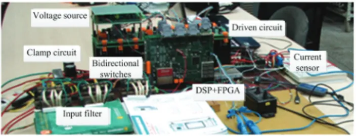
ESULTSA. Prototype of a Direct Three-Phase to Three-Phase MC
To demonstrate the validity of the proposed compensation method for grid side PF under unity control, a direct three- phase to three-phase MC prototype has been built in the laboratory as shown in Fig. 15. The experimental parameters are the same as the simulation parameters shown in Table II.
The prototype of the matrix converter is based on a DSP (TMS320F28335)+FPGA (EP2C8T144C8). The float-point DSP is used to fulfill the traditional SVPWM, the traditional and the proposed compensation methods. In addition, the FPGA is used to finish voltage-based on two-step commutation method and to generate the gating signals for the power circuit.
B. Experimental Results
The experimental results shown in Fig. 17 are the grid side and output waveforms of the MC at VTR=0.44, fo=15Hz under
different input filter parameters with the traditional SVPWM method. It can be seen that the grid side phase current leads the phase voltage since the effects of the input filter and the displacement angle between them are not different from those in Fig. 17(a) through Fig. 17(c). In Fig. 17(d) the displacement angle is increased when compared to Fig. 9(a). These results are identical to both the simulation results and the theoretical analysis.
Fig. 18 shows input/output waveforms of the MC with VTR
changing from VTR=0.44, fo=15Hz to VTR=0.58, fo=20Hz with
the traditional SVPWM method. With the output power increasing, the displacement angle between the grid side phase current and phase voltage is reduced. Therefore, the grid side PF can be improved by increasing the output power, which is identical to simulation results, verifying that the theoretical analysis is correct.
Fig. 19 shows input/output waveforms of the MC as VTR
changing from VTR=0.44, fo=15Hz to VTR=0.58, fo=20Hz with
the traditional compensation method and the proposed compensation method. As can be seen, both of the
0.15 0.2 0.25 -5 0 5 0.15 0.2 0.25 -10 0 10 IIs II II IIII II II IIs II bII IIII II II II II II Ih IIII III II A II II IIIIIIIhIIIIIIII bIIIIIIIhIIIIIIII 0.1 0.12 0.14 0.16 0.18 0.2 -2 0 2 0.1 0.12 0.14 0.16 0.18 0.2 -5 0 5 IIs II IIII IIII II III sII bIIII III III II III IIh III III II IA II II IIIIIIIhIIIIIIII bIIIIIIIhIIIIIIII 0.1 0.12 0.14 0.16 0.18 0.2 -5 0 5 0.1 0.12 0.14 0.16 0.18 0.2 -5 0 5 IIs II II III II II III Is I bI IIIIII IIII III II Ih II IIII II IA II II IIIIIIIhIIIIIIII bIIIIIIIhIIIIIIII
(a) (b)
(c) (d)
Fig. 17. Input/output waveforms with the traditional SVPWM at
VTR=0.44, fo=15Hz for: (a) Rf=50Ω, Lf=2mH, Cf=11.25µF, (b)
Rf=100Ω, Lf=2mH, Cf=11.25µF, (c) Rf=50Ω, Lf=4mH,
Cf=11.25µF, (d) Rf=50Ω, Lf=2mH, Cf=20µF.
.
Fig. 18. Input/output waveforms of the MC as the load changes from VTR=0.44, fo=15Hz to VTR=0.58, fo=20Hz with the
traditional SVPWM method.
(a) (b)
Fig. 19. Input/output waveforms of the MC as the load changes from VTR=0.44, fo=15Hz to VTR=0.58, fo=20Hz for the: (a)
Traditional compensation method, (b) Proposed compensation method.
compensation methods nearly achieve the goal of grid side PF under unity control, and the proposed compensation in the paper has a smaller displacement angle between the grid side phase current and the phase voltage than the traditional compensation method. Experimental results verify that both of the methods are feasible for achieving the grid side PF under unity control with a high VTR.
(a)
(b) (c)
Fig. 20. Input/output waveforms of the MC at VTR=0.22,
fo=7.5Hz for the: (a) Traditional SVPWM method, (b)
Traditional compensation method, (c) Proposed compensation method in this paper.
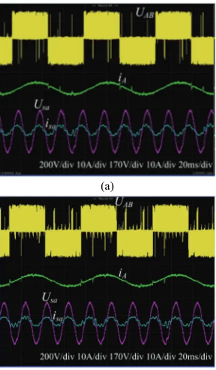
Fig. 20 shows input/output waveforms of the MC at the referenced output voltage VTR=0.22, fo=7.5Hz of the
traditional SVPWM method, the traditional compensation method, and the proposed compensation method under light load conditions. As can be seen, the grid side phase current leads the phase voltage with the traditional SVPWM method. With the traditional compensation method, the displacement angle between the grid side phase current and the phase voltage is decreased. However, they are still not in phase. With the proposed compensation method, the grid side phase current is almost in phase with phase voltage, and the grid side PF under unity control is achieved. However, the output voltage and the input current waveform qualities with the proposed compensation method are worse than those with the traditional compensation method. This is due to the fact that the proposed compensation method has a larger compensation angle than the traditional method. In other words, the angle of the input current vector with the proposed compensation method is modified to be higher than the conventional method. As a result, the input current harmonic with the proposed compensation method is higher than that with the conventional method. Even if the proposed input power factor compensation method has a higher PF in the light load condition, it is at the expense of the input performance of the MC.
Fig. 21 shows input/output waveforms of the MC at the referenced output voltage VTR=0.44 fo=15Hz and Cf =20µF
with both the traditional and the proposed compensation methods. As can be seen, with the proposed compensation method the grid side phase current is in phase with the phase voltage, and the displacement angle between them is slightly smaller than that with the traditional compensation method.
(a)
(b)
Fig. 21. Input/output waveforms of the MC at VTR=0.44, fo=15Hz
with Cf =20µF for the: (a) Traditional compensation method, (b)
Proposed compensation method.
These experimental results are identical to the simulation results, which verifies that the proposed method has better performance in terms of the grid side PF under unity control even if the filter capacity is increased.
In Fig. 17 through Fig. 21, UAB and iA are the output line
voltage and the output current, respectively. It can be seen that the output performances of the MC with the proposed method are slightly worse than those with the traditional method. This is due to the fact that the proposed method has a larger compensation angle than the traditional method, which leads to high harmonics in the input current. This in turn, worsens the output performances. A method to optimize the input and output performances under a high input power factor needs further study.
VI. C
ONCLUSIONIn this paper, the grid side PF, which is affected by the input filter parameters and the output power, was discussed. A new grid side PF under unity control was proposed by letting the reactive power be 0. The principal and maximum compensation angle of the proposed method implemented in indirect SVPWM were presented. Simulation results indicated that both the filter capacity and output power have a greater impact on the grid side PF. However, both the damping resistor and the filter inductance have less impact on the grid side PF. Simulation results also indicated that the proposed compensation method had better performances in terms of the grid side PF under unity control than that with the traditional compensation method. This was especially true
under light load conditions. However, this was at the expense of deteriorating the input current and output voltage waveform qualities. Experimental results verified that the theoretical analysis was correct and that the proposed compensation method was feasible.
R
EFERENCES[1] M. Siami, D. A. Khaburi, and J. Rodriguez, “Simplified finite control set-model predictive control for matrix converter-fed PMSM drives,” IEEE Trans. Power
Electron., Vol. 33, No. 3, pp. 2438-2446, Mar. 2018.
[2] T. D. Nguyen and H. H. Lee, “A new SVM method for an indirect matrix converter with common-mode voltage reduction,” IEEE Trans. Ind. Informat., Vol. 10, No. 1, pp. 61-726, Feb. 2014.
[3] Y. H. Xia, X. F. Zhang, and M. Z. Qiao, “An improved multi-orbit vector weighted over-modulation method of matrix converter,” Proc. the CSEE., Vol. 35, No.23, pp. 6143-6151, Dec. 2015.
[4] A. Trentin, P. Zanchetta, J. Clare, and P. Wheeler, “Automated optimal design of input filter for direct AC/AC matrix converter,” IEEE Trans. Ind. Electron., Vol. 59, No. 7, pp. 2811-2822, Jul. 2012.
[5] S. F. Pinto and J. F. Silva, “Input filter design for sliding mode controlled matrix converters,” in Proc. 32nd IEEE
Annu. Power Electron. Spec. Conf., Vol. 2, pp. 648-653,
2011.
[6] S. F. Pinto and J. F. Silva, “Direct control method for matrix converters with input power factor regulation,” in
Proc. 35th IEEE Power Electron . Spec. Conf., Vol. 3, pp.
2366-2372, 2004.
[7] T. Kume, K. Yamada, T. Higuchi, E. Yamamoto, H. Hara, T. Sawa, and M. M. Swamy, “Integrated filters and their combined effects in matrix converter,” IEEE Trans. Ind.
Appl., Vol. 43, No. 2, pp. 571-581, Mar./Apr. 2007.
[8] P. Siwek, “Input filter optimization for a DTC driven matrix converter-fed PMSM drive,” in Proc. 23th MMAR.
Conf., pp. 35-40, 2018.
[9] M. Rivera, M. Amirbande, and A. Vahedi, “Predictive control strategies operating at fixed switching frequency for input filter resonance mitigation in an indirect matrix converter,” in Proc. IEEE. Sou. Pow. Ele. Conf., pp. 1-6, Dec. 2017.
[10] A. K. Sahoo, K. Basu, and A. Mahan, “Systematic input filter design of matrix converter by analytical estimation of RMS current ripple,” IEEE Trans. Ind. Informat., Vol. 62, No. 1, pp. 132-143, Jan. 2015.
[11] D. Casadei, G. Serra, A. Tani, A. Trentin, and L. Zarri, “Theoretical and experimental investigation on the stability of matrix converters,” IEEE Trans. Ind. Electron., Vol. 52, No. 5, pp. 1409-1419, Oct. 2005.
[12] D. Casadei, G. Serra, and A. Tani, “Improvement of the stability of electrical drives fed by matrix converters,” in
Pro. IEEE Seminar on Matrix Converters, Birmingham,
U.K., pp. 3/1-3/12, 2003.
[13] D. Casadei, G. Serra, and A. Tani, “Effects on input voltage measurment on stability of matrix coverter drive system,” Proc. IEE-Electr-Electr. Power Appl., Vol. 151, No. 4, pp. 487-497, 2004.
[14] D. Casadei, J. Clare, L. Emprinham, G. Serra, A. Trentin, P. Wheeler, and L. Zarri, “Large-signal model for the stability
analysis of matrix converters,” IEEE Trans. Ind. Electron., Vol. 54, No. 2, pp. 939-950, Apr. 2007.
[15] N. Han, B. Zhou, and J. Yu, X. Qin, J. Lei, and Yang Yang, “A novel source current control strategy and its stability analysis for an indirect matrix converter,” IEEE Trans.
Pow. Eletron., Vol. 32, No. 10, pp. 8181-8192, Oct. 2017.
[16] Y. Sun, M. Su, and X. Li, H Wang, and W. H. Gui, “A general constructive approach to matrix converter stabilization,” IEEE Trans. Pow. Electron., Vol. 28, No. 1, pp. 418-441, Jan, 2013.
[17] L. Huber and D. Borojevic, “Space vector modulated three- phase to three-phase matrix converter with input power factor correction,” IEEE Trans. Ind. Appl., Vol. 31, No. 6, pp. 1234-1256, Nov. 1995.
[18] M. Rivera, C. Rojas, J. Rodriguez, P. Wheeler, B. Wu, and J. Espinoza, “Predictive current control with input filter resonance mitigation for a direct matrix converter,” IEEE
Trans. Power Electron., Vol. 26, No. 10, pp. 2794-2803,
Oct, 2007.
[19] H. M. Nguyen, H. H. Lee, and T. W. Chun, “Input power factor compensation algorithms using a new direct-SVM method for matrix converter,” IEEE Trans. Ind. Electron., Vol. 58, No. 1, pp. 232-243, Jan. 2011.
[20] R. Metidji, B. Metidji, and B. Metidji, “Design and implementation of a unity power factor fuzzy battery charger using ultrasparse matrix converter,” IEEE Trans.
Pow. Electron., Vol. 28, No. 5, pp. 2269-2276, May 2013.
[21] M. Rivera, J. Rodriguez, J. R. Espinoza, and H. Abu-Rub, “Instantaneous reactive power minimization and current control for an indirect matrix converter under a distorted AC supply,” IEEE Trans. Ind. Electron., Vol. 8, No. 3, pp. 482-590, Aug. 2012.
[22] M. Rivera, J. Rodriguez, and J. R. Espinoza, T. Friedli, J.W. Kolar, A. Wilson, and C. A. Rojas, “Imposed sinusoidal source and load currents for an indirect matrix converter,”
IEEE Trans. Ind. Electron., Vol. 59, No. 9, pp. 3427-3435,
Sep. 2012.
[23] F. Schafmeister and J. W. Kolar, “Novel hybrid modulation schemes significantly extending the reactive power control range of all matrix converter topologies with low computational effort,” IEEE Trans. Ind. Electron., Vol. 59, No. 1, pp. 194-210, Jan. 2012.
[24] X. Li, M. Su, and Y. Sun, H. B. Dan, and W. J. Xiong, “Modulation strategy based on mathematical construction for matrix converter extending the input reactive power range,” IEEE Trans. Power Electron., Vol. 29, No. 2, pp. 654-664, Feb. 2014.
[25] X. Li, Y. Sun, and J. X. Zhang, M. Su, and S. D. Huang, “Modulation methods for indirect matrix converter extending the input reactive power range,” IEEE Trans.
Power Electron., Vol. 32, No. 6, pp. 4852-4863, Jun. 2017.
[26] S. Mondal and D. Kastha, “Maximum active and reactive power capability of a matrix converter-fed DFIG-based wind energy conversion system,” IEEE J. Emerg. Sel.
Topics Power Electron., Vol. 5, No. 3, pp. 1322-1333, Sep.
2017.
[27] S. Mondal and D. Kastha, “Improved direct torque and reactive power control of a matrix-converter-fed grid- connected doubly fed induction generator,” IEEE Trans.
Ind. Electron., Vol. 62, No. 12, pp. 7590-7598, Dec. 2015.
[28] A. Yousefi-Talouki, E. Pouresmaeil, and B. N. Jorgensen, “Active and reactive power ripple minimization in direct power control of matrix converter-fed DFIG,” Int. J. Electr.
Power Energy Syst., Vol. 63, pp. 600-608, Dec. 2014.
[29] R. Cardenas, R. Pena, P. Wheeler, J. Clare, A. Munoz, and A. Sureda, “Control of a wind generation system based on a brushless doubly-fed induction generator fed by a matrix converter,” Electr. Power Syst. Res., Vol. 103, pp. 49-60, Oct. 2013.
[30] H. Hojabri, H. Mokhtari, and L. Chang, “Reactive power control of permanent-magnet synchronous wind generator with matrix converter,” IEEE Trans. Power Del., Vol. 28, No. 2, pp. 575-584, Apr. 2013.
[31] H. She, H. Lin, B. He, X. Wang, L. Yue, and X. An, “Implementation of voltage-based commutation in space- vector-modulated matrix converter,” IEEE Trans. Ind.
Eletron., Vol. 59, No. 1, pp.154-166, Jan. 2012.
Yihui Xia was born in Henan, China, in 1987. He received his B.S., M.S. and Ph.D. degrees in Electrical Engineering from the College of Electrical Engineering, Naval University of Engineering, Wuhan, China, in 2005, 2011 and 2015, respectively. He is presently working as a Lecturer in the College of Electrical Engineering, Navy University of Engineering. His current research interests include power electronics, electric machine drives, active power filters and matrix converters.
Zhihao Ye received his B.S., M.S. and Ph.D. degrees in Electrical Engineering from the College of Electrical Engineering, Naval University of Engineering, Wuhan, China, in 1997, 2000 and 2005, respectively. Since 2007, he has been working as a Professor in the College of Electrical Engineering, Navy University of Engineering. His current research interests include the automation of shipboard power systems.
Xiaofeng Zhang was born in Jiangsu, China, in 1963. He received his B.S. and M.S. degrees in Electrical Engineering from the College of Electrical Engineering, Naval University of Engineering, Wuhan, China, in 1982 and 1985, respectively. He received his Ph.D. degree from Tsinghua University, Beijing, China, in 1996. Since 1997, he has been working as a Professor in the College of Electrical Engineering, Navy University of Engineering. His current research interests include the automation of shipboard power systems.
Mingzhong Qiao was born in Jiangsu, China, in 1971. He received his B.S., M.S. and Ph.D. degrees in Electrical Engineering from the College of Electrical Engineering, Naval University of Engineering, Wuhan, China, in 1996, 1999 and 2003, respectively. Since 2012, he has been working as a Professor in the College of Electrical Engineering, Navy University of Engineering. His current research interests include power electronics and electric machine drives.