2017년 12월
17ZB1100
50
나노전자원 기술연구
본 문서에서 음영처리된 부분은 (
) 정보공개법 제9조의 비공개대상정보와 저
작권법 및 그 밖의 다른 법령에서 보호하고 있는 제3자의 권리가 포함된 저작물로 공
개대상에서 제외되었습니다.
제 출 문
본 연구보고서는 일반사업 연구과제인 "나노 전자원 기술 연구"의 결과로서, 본 과제에 참여한 아래의 연구팀이 작성한 것입니다. 2017년 12월 08일 연구책임자 : 책임연구원 송윤호 (신소자연구그룹장) 연구참여자 : 책임연구원 이진호 (소재부품원천연구본부장) 연구참여자 : 책임연구원 정진우 (신소자연구그룹) 연구참여자 : 선임연구원 최영철 (신소자연구그룹) 연구참여자 : 선임연구원 강준태 (신소자연구그룹) 연구참여자 : 선임연구원 김재우 (신소자연구그룹) 연구참여자 : 선임연구원 박소라 (신소자연구그룹) 연구참여자 : 연 수 생 전효진 (신소자연구그룹) 연구참여자 : 연 수 생 고은솔 (신소자연구그룹) 연구참여자 : 연 수 생 이정웅 (신소자연구그룹) 연구참여자 : 특수계약직 연지환 (신소자연구그룹) 연구참여자 : 특수계약직 김성희 (신소자연구그룹) 연구참여자 : 위촉연구원 윤효은 (신소자연구그룹)세부과제 연차실적 보고서
연차실적 보고서
과제유형
1. 기초미래선도형 ( ㅇ ) 2. 공공인프라형 ( ) 3. 산업화형 ( )
대과제명
ICT소재부품 기초·원천 기술개발
세부과제명
나노 전자원 기술 연구
세부과제
책임자
소속 및 부서
신소자연구그룹
직위
(직급)
그룹장
성명
송윤호
총연구기간
2015년 01월 01일 부터 2017년 12월 31일 까지 (36개월)
당해연도
연구기간
2017년 01월 01일 부터 2017년 12월 31일 까지 (12개월)
총
연
구
비
정부출연금
2,731,013 천원
당
해
년
연
구
비
정부출연금
889,000 천원
민간부담금
천원
민간부담금
천원
계
2,731,013 천원
계
889,000 천원
참여인력(M/Y)
총 연 구 기 간
44 명 ( 6.5 M/Y)
당해연도 연구기간
13 명 ( 4.9 M/Y)
참여기관
기관명
연구책임자
기관명
연구책임자
참여연구기관
위탁연구기관
고려대학교 이철진키워드
(6~10개)
탄소나노튜브, 전계방출 전자원, 엑스선 소스,
정부출연금사업 연차평가 보고서를 제출합니다.
2017 년 12 월 08 일
세부과제책임자 : 송 윤 호 (인)
요 약 문
Ⅰ. 제 목
나노 전자원 기술 연구Ⅱ. 연구목적 및 중요성
¤ 연구 목적 본 과제의 목적은 기존 전자소스의 한계를 뛰어넘는 신개념의 초고밀도 나노 전자원(nano electron source)을 개발하고, 이를 적용한 신개념 의료 영상/치료, 실시간 보안검색 등 획기적 응용기술과 산업창출에 있다. ¤ 연구의 중요성 기존의 전자원은 가열(heating), 광-여기(photo-excited), 또는 전계 방출(field emission) 방법으로 얻는데, 이러한 종래 전자원은 전자방출의 효율과 방출 밀도가 낮아 응용 분야가 제한적이다. 이러한 단점을 극복하기 위해 본 과제에서 개발하는 초고밀도 나노 전자원은 나노 크기 및 구조의 물질로부터 양자역학적 극한의 밀도로 전자를 진공으로 방출시켜 얻는 신개념의 초극소형, 고전류 전자원(原)을 일컬으며, 이를 이용하여 전자방출 효율과 전류밀도를 획기적으로 증가시켜 전자원의 응용 분야 확대가 가능하다. 또한 초고밀도 나노 전자원은 기존의 아날로그 엑스선 소스를 초소형화, 디지털화할 수 있기 때문에 근접치료 시스템, 단층영상합성(tomosynthesis) 시스템, 스마트·포터블 CT와 같은 혁신적인 신개념의 의료영상 및 치료 시스템의 시장을 창출하여 경제적 효과가 매우 클 것으로 기대되며, 새로운 의료 시스템 제공으로 인간의 삶의 질 향상에 크게 기여할 수 있다.Ⅲ. 연구내용 및 범위
§ 1D/2D 나노물질 기반 고밀도 전자원 연구 - 2D 나노물질 기반 전자투과 및 자기집속형 게이트 연구 - 1D/2D 나노물질 기반 초고밀도 전자원 제작 및 분석 - 초고밀도 나노전자원 기반 디지털 엑스선 튜브 개발 § 신개념의 행렬-어드레싱형 엑스선 소스 제작 및 평가 - 신개념 행렬어레이 엑스선 소스 제작 - 행렬-어드레싱형 엑스선 구동 시스템 개발 - 행렬 엑스선 선량 및 관전류 특성 평가Ⅳ. 연구결과
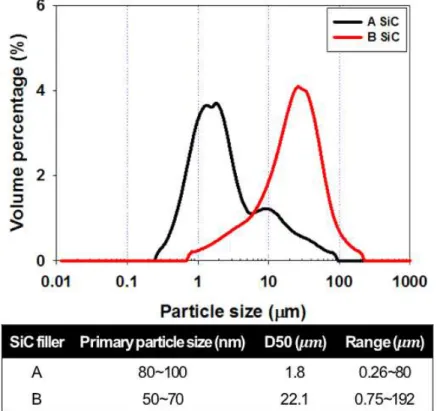
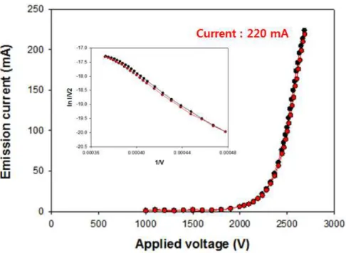
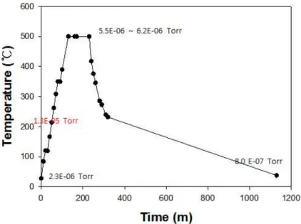
초고밀도 나노 전자원 및 신개념 행렬-어드레싱형 엑스선 소스 연구를 수행하여 다음과 같은 우수한 연구결과를 도출하였다. 본 과제에서는 우수한 특성의 고전류밀도 전자원 개발을 위해 CNT 재료를 기반으로 페이스트 에미터를 제작하였다. 이 때, 페이스트 에미터의 기판 접착 특성과 밀접하게 연관된 무기필러 나노파우더의 응집 특성을 분석하고 미니밀 분쇄 방법을 통해 입도 분포를 제어하여 에미터의 고전류 전계방출 안정성을 크게 향상시켰고, 220 mA 의 고전류 방출 특성을 달성하였다. 우수한 특성의 CNT 기반 전자원으로부터 양자역학적 극한의 초고밀도 전류 방출 특성을 확보하기 위해 본 과제에서는 상대적으로 작은 직경으로 제작이 용이한 CNT-yarn을 사용한 나노전자원을 제작하여 전계방출 특성을 분석하였다. 직경이 약 30 µm, 길이 300 µm 의 CNT-yarn 에미터로부터 200 A/cm2 이상의 초고전류밀도 특성을 달성하였다. 이러한 극소단면 CNT-yarn 에미터는 완전 진공 밀봉된 튜브에서 전류밀도 22 A/cm2, 연속 160 시간의 매우 안정적인 전계방출 특성을 보였다. 2D 나노물질인 그래핀을 진공 고온 열처리를 통해 게이트 개구 위에 전사하는 기술을 개발하여 전자투과형 자기집속 게이트(ETANG : Electron transmissiveatomic network gate)를 개발하였으며, 전사된 다층 그래핀의 표면 형상과 물성을 심화 연구하여 전계방출 소자에 적용되었을 때 전자 빔의 경로와 집속도에 어떤 영향을 미치는지 시뮬레이션을 통해 확인하였다. 또한 그 결과를 바탕으로 ETANG 구조의 최적화 방향을 설정하였다. 개발된 초고밀도 나노 전자원을 기반으로 진공 밀봉 형태의 디지털 엑스선 튜브(PXT)를 제작하였고, 40개의 엑스선 튜브를 사용하여 8×5 행렬-어드레싱형 엑스선 소스를 제작하였다. 최대 관전압 50 kV, 단위소스당 선량 1 mAs(전류기준), 관전류 5 mA (최대 10 mA) 이상의 조건에서 안정적인 구동이 가능한 엑스선 소스를 개발하였다. 개발된 신개념 엑스선 소스의 엑스선 방출 면적은 15 ×24 cm2를 달성하였다. 또한 아두이노-메가 기반의 40 채널 구동 모듈 및 제어 프로그램을 제작하여 임의의 PXT를 원하는 시간에 구동할 수 있게 하였다. 구동 특성 평가를 위해 3×3 PXT 배열의 순차, 2-shots 및 4-shots 구동이 가능함을 확인하였다.
¤ 목표대비 달성도 성과지표 당해 연도 목표 성과 달성도 초고밀도 전자원 기술 전류밀도 : 20 A/cm2 22 A/cm2 > 100 % 전류 : 0.2 A 0.22 A > 100 % 신개념의 행렬-어드레싱형 엑스선 소스 기술 엑스선 방출 면적 : 15 x 10 cm2 15 x 24 cm2 > 100 % 행렬어레이 : 8 x 5 8 x 5 100 % 관전류 : 5 mA 10 mA > 100 % 계량지표 SCI 논문게재: 4편 (IF상위20% 2편) SCI 3편 (IF상위20% 3편) 국제학회 초청발표: 2건 150 % (IF 기준) 국내외 특허: 각 3건(3극 출원 1건) 국내 : 4건 국외 : 4건 100 % ¤ 추가 성과 성 과 내 용 기술이전 사업화 주요사업 성과로 2015년에 이전된 기술(나노 전계에미터 및 디지털 엑스선 튜브)이 포터블 덴탈 엑스선 장치(상품명: EzRay Air & EzRay Air
W)로 국내, 외에 사업화되기 시작함 기술이전 : 1건 기술이전 1건(산업용 디지털 엑스선 튜브 기술) 추진 중임 신규과제수주 : 1건 주요사업의 핵심기술 및 확보된 지식재산권을 바탕으로 한국연구재단 방사선기술개발사업 신규과제 수주(“고속, 가변 프레임의 디지털 엑스선 소스에 의한 엑스선 투시 영상 시스템 기술 개발”; 3년, 5억원/년)
Ⅴ. 연구개발결과의 활용계획
본 과제에서 개발한 초고밀도 나노 전자원 개발을 이용하여 종래의 전자원을 대체하고, 이로 부터 기존 전자원 제품의 디지털화, 소형화, 경량화, 저전력화 및 혁신적인 품질 개선을 달성할 계획이다. 초고밀도 나노 전자원은 극소형, 고전류 특성을 지니기 때문에 초소형 디지털 엑스선 소스, 스마트·포터블 CT, 고품위 조명 램프, 포터블 물성 분석기, 엑스선 현미경 등 새로운 응용분야에 디지털 엑스선 소스로 활용이 가능할 것으로 기대된다.Ⅵ. 기대성과
초고밀도 나노 전자원은 기존 전자원의 물리적 한계를 뛰어넘는 초소형, 고전류 및 고휘도 전자원(電子原) 영역의 새로운 분야를 개척하는 기술적 효과가 기대된다. 초고밀도 나노 전자원은 기존 전자빔 제품의 소형화 및 고성능화와 더불어 초소형 디지털 엑스선 소스, 테라헤르츠파 소스, 스마트·포터블 CT, 고품위 조명 램프, 포터블 물성 분석기, 엑스선 현미경과 같은 새로운 응용 산업 및 시장의 창출이 가능하므로 그 경제적 효과가 매우 클 것으로 기대된다. 선진국 대비 뒤떨어진 국내의 전자원 관련 의료, 보안 및 검색 기술을 크게 선진화시킬 수 있을 뿐만 아니라 아직까지 세계적으로 구현되지 않은 혁신적인 기술과 제품을 개발함으로써 나노 전자원의 글로벌 리더쉽을 확보할 수 있다. 본 과제에서 성공적으로 개발된 초고밀도 나노 전자원은 초소형 디지털 의료 영상 및 치료원 소자 그리고 신개념의 행렬-어드레싱형 엑스선 소스에 적용하여 그 가능성을 타진하고, 이를 바탕으로 국내 관련업체에 기술이전을 추가로 추진할 계획이다.ABSTRACT
Ⅰ. TITLE
A study on the technology of nano electron-source
Ⅱ. THE OBJECTIVE AND IMPORTANCE OF THE STUDY
¤ OBJECTIVE
The conventional electron sources based on heating, photo-exciting, and field emission have suffered from low current density because of limited emission efficiency. The objective of this study is to develop novel ultra-high current density nano-electron source that overcomes the limitation of current electron source. It is intended to expand the applications of field emission as well as creating novel innovative technologies and industries.
¤ IMPORTANCE OF THIS STUDY
To solve the problems from which the conventional electron sources suffer, we have developed a nanomaterial-based miniature electron source that is able to generate ultra-high current density with quantum degeneracy. Because this novel electron source increases the emission efficiency and current density markedly, it can be used in various application fields including digital x-ray source, tomosynthesis system, brachytherapy, smart/portable CT, and so on. Therefore, the ultra high current density nano-electron source is expected to open a new era in the
market of medical imaging and therapy, which will create the new commercial market. Hence, the quality of human life is expected to be improved with this novel device.
Ⅲ. THE CONTENTS AND SCOPE OF THE STUDY
§ Study on the 1D/2D nanomaterials-based high current density electron source
- Study on the 2D nanomaterial-based electron transparent focusing gate - Fabrication and characterization of 1D/2D nanomaterials-based high current density electron source
- Development of digital x-ray tube using ultra-high current density nano-electron source
§ Fabrication and evaluation of new-concept matrix-addressable x-ray source
- Fabrication of new-concept matrix-array x-ray source - Development of matrix-addressable x-ray system
Ⅳ. RESULTS
We have studied on the ultra-high current density nano-electron source and new-concept matrix-addressable x-ray source, and achieved meaningful results, as follows.
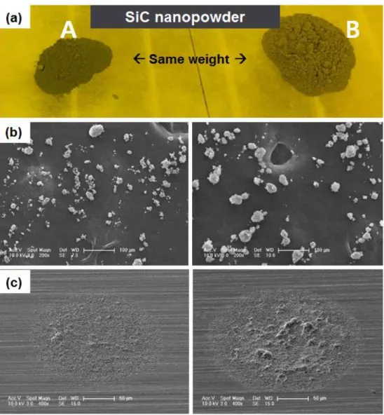
A paste emitter was fabricated on the basis of CNT material for developing a high current density electron source with excellent characteristics. The aggregation characteristics of the inorganic filler nano powder closely related to the substrate adhesion characteristics of the paste emitter were analyzed and the grain size distribution was controlled by the mini milling method to greatly improve the high current field emission stability of the emitter and achieve a high current emission characteristic of 220 mA.
In order to achieve quantum mechanical extreme ultra-high density current emission characteristics from CNT-based electron sources with excellent characteristics, we fabricated a CNT-yarn emitter with relatively small emission area and analysed its field emission characteristics. Ultra-high current densities of over 200 A/cm2 were
obtained from a CNT-yarn emitter with a diameter of about 30 μm and a length of 300 μm. Very small cross-section CNT-yarn emitters exhibited a very stable field emission characteristic with a current density of 22 A/cm2 and a continuous operation of 160 hours in a fully vacuum-sealed
tube.
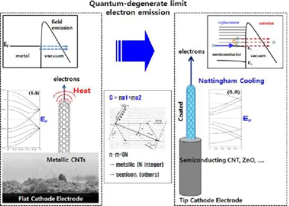
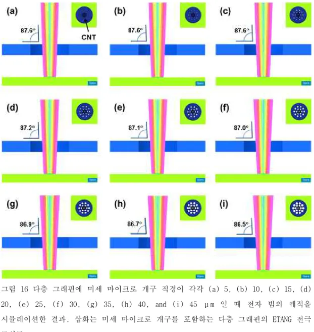
Electron transmissive atomic network gate (ETANG) has been developed by a technique to transfer graphene, a 2D nano material, to the gate opening through vacuum high-temperature annealing. By studying the surface morphology and physical properties of the transferred multi-layer graphene, we have confirmed how those affects electron beam path and when applied to field emission devices. Based on the results, optimization
direction of the ETANG structure was established.
Based on the developed ultra-high density nanoelectron source, a vacuum sealed digital X-ray tube (PXT) was fabricated and an 8×5 matrix-addressed x-ray source was produced using 40 x-ray tubes.
We developed an X-ray source capable of stable operation with a maximum tube voltage of 50 kV, dose per unit source of 1 mAs (current basis), and tube current of 5 mA (maximum 10 mA). The X-ray emission area of the new concept X-ray source was 15×24 cm2. In addition, a 40-channel drive
module and a control program based on Arduino-mega have been made to enable arbitrary PXT to be driven at a desired time. It was confirmed that sequential, 2-shots and 4-shots driving of the 3×3 PXT array is possible for driving characteristics evaluation.
¤ Quantitative achievements
Item Annual target (’17 Achievement Percentage High-density nano-electron source Current density : 20 A/cm2 22 A/cm2 > 100 % Current : 0.2 A 0.22 A > 100 % Matrix-addressable x-ray source x-ray area : 15 x 10 cm2 15 x 24 cm2 > 100 % Matrix-array : 8 x 5 8 x 5 100 % Tube current : 5 mA 10 mA > 100 % Publication SCI paper: 4 (IF >20%: 2) SCI paper: 3 (IF >20%: 3) Invited talk in international converence: 2 150 % (based on IF) IP applications : Domestic 3, Overseas 3 (triadic: 1) Domestic 4 Overseas 4 100 % Item Contents Technology commercialization : 1
The transfered technology (nano field emitter and digital x-ray tube) based on the achievement of this project in 2015 is commercialized in domestic and overseas with a
portable dental X-ray device (Product name: EzRay Air & EzRay Air W)
Technology transfer
: 1
1 technology transfer (industrial digital x-ray tube technology) (in progress)
New project orders : 1
Based on the results from this project, a new project of “Development of Fluoroscopic Imaging System Using Fast and Variable Frame
Rated Digital X-ray Sources”(Total project duration 3 years, 500 million won/year) is
Ⅴ. FUTURE PLAN FOR UTILIZING RESEARCH RESULTS
The ultra-high current density nano-electron source fabricated in the study will be used to develop digital, low-weight, miniature, and low power consumption electron source. Because of its very small size and high current capability, the ultra-high current density nano-electron source will be used in various application fields, such as super-miniature x-ray source, smart/portable CT, high y lamp, portable analysis tools, x-ray microscope, etc.
Ⅵ. RESEARCH ACHIEVEMENTS
The ultra-high current density nano-electron source is believed to overcome the limited performance of conventional electron source, so that it is expected to open a new era of super-miniature, high current, and high brightness electron source. Therefore, the nano-electron source has a big potential to create new industry and market related to miniature x-ray tube, tera-Hz source, smart/portable CT, high quality lamp, portable analysis tools, x-ray microscope, etc.
Not only can the nano-electron source facilitate the domestic medical and security industries, but it will also make possible to have global leadership in electron source industry by innovative technologies and products.
The ultra-high current density nano-electron source which is successfully developed through this project is going to be used in developing miniature digital medical imaging/therapy system and new concept matrix addressable x-ray source. Additionally, we will attempt to licence this technologies in domestic corporations.
CONTENTS
CHAPTER 1 Introduction
1
SECTION 1 Research goals
1
SECTION 2 Research content
1
SECTION 3 Research method
2
SECTION 4 Reporting System
3
CHAPTER 2 Main contents (Ⅰ)
4
SECTION 1 Necessity of research and development task
4
1. Background and Necessity
4
2. Importance of research projects
5
A. Economic importance
5
B. Social and cultural importance
7
3. Constraints of research project performance
8
4. Expected effects of research tasks
8
SECTION 2 Status and Approach
10
1. Domestic and Foreign Status
10
A. Domestic technology trends and levels
10
B. Overseas technology trends and levels
10
C. Domestic and foreign standardization status
11
D. Performances of domestic and foreign related persons on the
same and similar contents
12
E. Project or research project already carried out by the
proponent in relation to the same or similar contents
12
F. Domestic and foreign competitors
13
G. Domestic and foreign intellectual property rights
15
2. Key elements and approach of research project
16
CHAPTER 2 Main contents (Ⅱ)
18
SECTION 1 Research objectives and contents
18
1. Final research objectives and contents
18
2. Research objectives and contents of the year
19
SECTION 2 Research plans and performance
20
1. Research plan
20
2. Research performance
22
A. Outline of research performance
22
B. Performance indicators and goals
23
C. Technology development and research output achievement
24
3. Outline of research results
30
SECTION 3 Results
31
1. Research on high current density electron source based on 1D /
2D nanomaterials
31
A. Study of electron transmission and self-focusing gate based
B. 1D Carbon Nanotube (CNT)-based nano electron source research
40
C. Production and analysis of 1D / 2D nanomaterial-based high
current density electron source
61
2. Development and evaluation of new concept matrix-addressing
x-ray source
77
SECTION 4 Research output
95
CHAPTER 3 Plan to utilize research results
115
CHAPTER 4 Conclusion
117
CHAPTER 5 Research Facilities and Equipment Status
119
Reference
121
Tables
Table 1. Status of Overseas Competition Agencies 13 Table 2. Domestic Competition Agencies 14 Table 3. Step-by-step goals 18 Table 4. Research Promotion System 20 Table 5. Technical development performance index 23 Table 6. Research output performance index 23 Table 7. Achievement versus goal 24 Table 8. Additional achievements 24
·