26-4 / M. K. Ryu
• IMID 2009 DIGEST
Abstract
Highly stable bottom gate thin film transistors(TFTs) with a zinc indium tin oxide(Zn-In-Sn-O:ZITO) channel layer have been fabricated by rf-magnetron co-sputtering using a indium tin oxide(ITO:90/10), a tin oxide and a zinc oxide targets. The ZITO TFT (W/L=40μm/20μm) has a mobility of 24.6 cm2/V.s, a subthreshold swing of 0.12V/dec., a turn-on voltage of -0.4V and an on/off ratio of >109. When gate field of 1.8 x 10⁵ V/cm was applied with source-drain current of 3μA at 60oC, the threshold voltage shift was ~0.18 V after 135 hours. We fabricated AM-OLED driven by highly stable bottom gate Zn-In-Sn-O TFT array.
1. Introduction
Transparent oxide thin film transistors (TFTs) hold great promise for a variety of electronic applications, including active-matrix (AM) liquid crystal displays, organic light-emitting diode (OLED) displays1, and flexible and/or
see-through displays, because they not only have high mobility but also can be fabricated uniformly at low temperature in a large-area with a low production cost. For the display application, the stability requirement is more stringent for driving OLED than for driving AMLCD. In AMLCDs, the TFT functions as a digital switch with a low duty cycle (~0.1%), and a threshold voltage (Vth) shift of a few volts
can be tolerated2. In AMOLED pixels, however,
an increase of the Vth of the driving TFT reduces
the OLED driving current to decrease the brightness of the pixel. Therefore, it is very important to get high stability of TFT under bias stress with high mobility. Here we report highly stable bottom gate ZITO TFTs that is superior to any other oxide TFT. Furthermore, we fabricated transparent ZITO TFT (TTFT) array and integrated OLED on the TTFT array to result in
high aperture ratio of 2.5” bottom emission AM-OLED.
2. Experimental
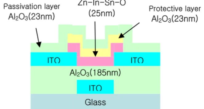
We have fabricated the bottom gate TFTs with the active layer composed with Zn-In-Sn-O (ZITO). The schematic diagram of the bottom gate ZITO TFT structure is shown in Fig. 1. An alkaline-free glass was used as a substrate. Gate and source/drain electrodes were deposited with 150 nm-thick ITO (indium tin oxide). A gate insulator of Al2O3
was formed by atomic layer deposition (ALD) method at 150 oC and its thickness was 180 nm. A ZITO layer
was formed by co-sputtering of an ITO(90:10), a SnO2
and a ZnO targets with an off-axis type RF magnetron sputter at room temperature. The sputtering was performed in the atmosphere of Ar and O2 mixed gas
with the chamber pressure of 0.3 Pa. The protective layer and passivation layer were 23 nm-thick Al2O3
deposited by PEALD method using trimethyl aluminum (TMA) and oxygen plasma. All patterning processes were performed by photo-lithographic method and wet etching process. The annealing was performed at 300oC in O
2 atmosphere. The electrical
characteristics of the TFTs were measured with the semiconductor parameter analyzer (Agilent B1500A) in darkness.
Fig. 1. Cross sectional view of bottom gate ZITO TFT.
Glass ITO ITO ITO Zn-In-Sn-O (25nm) Protective layer Al2O3(23nm) Passivation layer Al2O3(23nm) Al2O3(185nm)
Highly stable Zn-In-Sn-O TFTs for the Application of
AM-OLED Display
Min Ki Ryu*, Sang-Hee Ko Park, Shin Hyuk Yang, Woo-Seok Cheong,
Chun-Won Byun, Sung Mook Chung, OhSang Kwon, Eunsuk Park, Jae
Kyeong Jeong, Kyoung Ik Cho, Doo-hee Cho
a, Jeong-Ik Lee
a, and Chi-Sun
Hwang
Transparent Display Team, OLED Lighting Teama, ETRI, Daejeon 305-700, Korea
26-4 / M. K. Ryu
IMID 2009 DIGEST •
3. Results and Discussion
Fig. 2 shows the transfer characteristics of the ZITO TFT. The measurement was carried out by varying the VGS value from -10V to 20V and then back to -10V.
An excellent SS of 0.12V/decade, Von of -0.4V, and
high on/off ratio of >109 as well as a high µ
FE of 24.6
cm2/Vs were achieved.
Fig. 2. The transfer characteristics of the ZITO TFT(W/L=40μm/20μm). The measurement was carried out by varying the VGS value from -10V to
20V and then back to -10V.
To measure bias stress stability, we applied gate voltage was 3.5 V with source-drain currents of 3µA at 60oC which is sufficient to provide drain current required to drive a typical OLED pixel.
In Fig. 3(a), bias stressing was interrupted in order to measure the transfer characteristics. Saturation mobility µFE and Vth were obtained in the saturation
regime by extracting the axis intercept and the slope above Vth from ID0.5 vs VG plot, respectively. The
same slopes for the 0 second, 100K seconds, and 135 hours means that the mobility is almost unchanged during bias stress. Considering most of oxide TFTs with high mobility showed change of mobility under bias stress due to the defects creation in the active bulk film, our ZITO active film seems to be relatively stable. In Fig. 3(b) the time dependence of ∆Vth for selected
samples is presented on a logarithmic time scale. Transfer curve shifted to positive way under bias stress. We are under investigation to clarify the mechanism of Vth shift under bias stress.
FIG. 3. (a) ID0.5 vs VG plot used to extract Vth, ∆Vth,
and µFE during bias stress test at 60oC and (b) the
corresponding time dependencies of ∆Vth for selected
samples.
3. Impact
We developed that high stable bottom gate oxide TFT. The ZITO TFTs(W/L=40m/20µm) has a mobility of 24.6 cm2/V.s, a subthreshold swing of 0.12V/dec., a
turn-on voltage of -0.4V and an on/off ratio of >109.
When operated at a gate filed of 1.8 x 10⁵ V/cm with
source-drain currents of 3µA, the Vth shift is ~0.18 V after 135 hours at 60oC. While most of oxide TFT
with mobility higher than 15 cm2/V.s showed
relatively poor bias stress stability, our ZITO TFTs have excellent stability even with high mobility. We will demonstrate AM-OLED with ZITO TFT.
(a)
26-4 / M. K. Ryu
• IMID 2009 DIGEST
5. Acknowledgement
This work was supported by the IT R&D program of MIC/IITA. [2006-S079-04, Smart window with transparent electronic devices].
6. References
1. Sang-Hee Ko Park, Chi-Sun Hwang, Leong-Ik Lee, Sung Mook Chung, Yong Suk Yang, Lee-Mi Do, and Hye Yong Chu, Proc. SID’06, p 25, 2006. 2. Bahman Hekmatshoar, Kunigunde H. Cherenack,
Alex Z. Kattamis, Ke Long, Sigurd Wagner, and James C. Sturm, Appl. Phys. Lett. 93, 032103 (2008).