https://doi.org/10.6113/JPE.2019.19.6.1486 ISSN(Print): 1598-2092 / ISSN(Online): 2093-4718
JPE 19-6-14
Hybrid Double Direction Blocking Sub-Module for
MMC-HVDC Design and Control
Jianpo Zhang
†, Diqiong Cui
*, Xincheng Tian
*, and Chengyong Zhao
*†,*State Key Laboratory of Alternate Electrical Power System with Renewable Energy Sources, North China Electric Power University, Baoding, China
**Tangshan Power Corporation of China State Grid, Tangshan, China
Abstract
Dealing with the DC link fault poses a technical problem for an HVDC based on a modular multilevel converter. The fault suppressing mechanisms of several sub-module topologies with DC fault current blocking capacity are examined in this paper. An improved half-bridge sub-module topology with double direction control switch is also designed to address the additional power consumption problem, and a sub-module topology called hybrid double direction blocking sub module (HDDBSM) is proposed. The DC fault suppression characteristics and sub-module capacitor voltage balance problem is also analyzed, and a self-startup method is designed according to the number of capacitors. The simulation model in PSCAD/EMTDC is built to verify the self-startup process and the DC link fault suppression features.
Key words: DDCS, HDDBSM, Self-startup, Voltage balance
I. I
NTRODUCTIONTo achieve DC fault suppression, a high-voltage direct current transmission based on a modular multi-level converter (MMC-HVDC) must be able to cut off the fault current path from the AC side to the DC side and dissipate inductance storage energy. The MMC sub-module topologies shown in Fig. 1 can be classified into three types based on their fault current suppression mechanisms. First, active self-blocking fault suppression topologies include the full bridge sub-module (FBSM), single pole full bridge sub-module (SPFBSM), clamp diode double sub-module (CDSM), series double sub-module (SDSM), and cross three-level sub-module (CTL), all of which use the capacitor charging effect to absorb part of the energy in the fault loop and provide reverse voltage to turn the diode into a reverse bias state [1]-[13]. Second, passive inhibition topologies cut off the AC feeding current path and separate the AC and DC sides by using a double parallel
thyristor bypass circuit. These topologies achieve fault suppression by using a resistor in the loop to absorb the short circuit energy [14]. These topologies have been labeled passive inhibition topologies given their lack of an energy absorption capacitor and their use of resistors for energy dissipation. Third, shutdown sub-module topologies, such as the self-blocking sub-module topology illustrated in Fig. 1(h), utilize switches to directly cut off the arm current. These topologies can achieve a DC fault suppression effect but are relatively more problematic compared with simple half-bridge sub-modules.
For active self-blocking fault suppression topologies, the number of power devices and the additional conduction losses continue to increase as clamp switches are used to change the arm current direction and charge capacitors. To address this problem, a hybrid topology based on active self-blocking and HBSM is proposed as shown in Fig. 1(c). However, this hybrid topology faces an unbalanced capacitor charging problem.
By contrast, passive inhibition topologies do not suffer from the additional losses problem. However, if the DC link fault clearing time is long and the DC line fault cannot be cleared before the AC circuit breaker is triggered, then the AC circuit breaker cuts off the fault current. Shutdown sub-module topologies also face several problems, including
© 2019 KIPE Manuscript receivedJun. 17, 2018; accepted Aug. 26, 2019
Recommended for publication by Associate EditorJong-Pil Lee.
†Corresponding Author: zhangjianpo@126.com
Tel: +86-13933970921, North China Electric Power University
*State Key Laboratory of Alternate Electrical Power System with Renewable
Energy Sources, North China Electric Power University, China
(a) (b) (c) (d)
(e) (f) (g) (h)
Fig. 1. Different sub-module topologies. (a) FBSM. (b) SPFBSM. (c) SPFBSM+HBSM. (d) Double parallel thyristor sub-module. (e) CDSM. (f) SDSM. (g) CTSM. (h) Self-cutting off sub-module.
the huge energy and power consumption and the possible overvoltage while turning off.
This paper addresses the MMC–HVDC DC link current suppression issues by presenting an improved half-bridge topology and a hybrid sub-module topology based on double direction control switches (HDDBSM), by analyzing the DC link fault suppression characteristics and the unbalanced charge problem, by designing a self-startup strategy, and by verifying the effectiveness of the DC fault suppression and control strategy of the proposed topology in a PSCAD/ EMTDC environment.
This paper is organized as follows. Section II analyzes the half-bridge sub-module problem and designs HDDBSM. Section III presents the inhibition characteristics of HDDBSM, analyzes the capacitor voltage unbalanced problem, and designs the self-starting strategy. Section IV presents the simulation results for the control strategy of HDDBSM- HVDC and DC link fault blocking capacity. Section V presents the concluding remarks.
II. H
DDBSMD
ESIGN ANDA
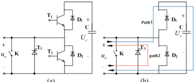
NALYSISWhen the half-bridge sub-module shown in Fig. 2 is locked, path2 sends this sub-module to the bypass state as a result of the D2 freewheeling effect, and the AC side continuously feeds fault current to the DC net. In this sense, this sub-module lacks a DC fault suppression capability.
Given that the uncontrollability of diode D2 creates a fault suppression problem in path2, if D2 is replaced by a double direction controllable switch (DDCS), then path2 is cut off under the DC link fault. Several DDCS topologies are illustrated in Fig. 3 [15]-[18]. The first topology comprises four diodes and one IGBT (T). When T is locked, the double direction current can be blocked. However, three devices are present in the conduction path, and this DCCS topology is applied in the DC circuit breaker. The second topology comprises back-to-back connected IGBTs without the associated freewheeling diodes that are not connected in parallel but in series. The third topology, which is a bidirectional switch
(a) (b)
Fig. 2. HBSM and arm current path after blocking. (a) HBSM. (b) Arm current path.
(a) (b) (c) (d)
Fig. 3. DDCS topologies. (a) IGBT with diodes H bridge. (b) Anti-parallel IGBT without series diodes. (c) Common emitter topology. (d) Anti-parallel RBIGBT.
topology, comprises back-to-back connected IGBTs with freewheeling diodes as shown in Fig. 3(c) and is called the common emitter topology [18]. The main drawback of this switch arrangement is that a significant on-state voltage occurs as a result of the series connection between two devices (i.e., an IGBT and a diode). To solve this problem, a new bidirectional switch called reverse blocking IGBT (RBIGBT) has been introduced in the literature [15]-[18]. RBIGBT is a specific IGBT that can withstand voltage from both directions. The bidirectional switch is arranged as an anti-parallel connection of two RBIGBTs as shown in Fig. 3(d). Using these devices in MMC may reduce the operation power loss due to the low on-state conduction losses of the semiconductors. The topology shown in Fig. 3(c) is applied as a load commutation switch in an ABB hybrid HVDC breaker [19], whereas that shown in Fig. 3(d) is mainly used in low- and middle-voltage T-type converters. These two topologies can also be used as DDCS in the MMC sub-module.
c U Uc o u o u
(a) (b)
Fig. 4. HDDBSM with different DCCS. (a) Common emitter topology (HDDBSM_1). (b) Anti-parallel RBIGBT (HDDBSM_2).
(a) (b)
Fig. 5. HDDBSM with a blocked current path. (a) When the current is positive. (b) When the current is negative.
TABLE I SWITCH STATES OF HDDBSM Working states T1 T2 T3 T4 T5 U0 SM1 inserted 1 0 0 1 1 Uc1 SM2 inserted 0 1 1 0 0 Uc2 SM1SM2 bypassed 0 1 0 1 1 0
SM1SM2 inserted 1 0 1 0 0 Uc1+ Uc2
Both blocked (i>0) 0 0 0 0 0 Uc1+ Uc2 Both blocked (i<0) 0 0 0 0 0 -Uc1
Moreover, the topologies in Figs. 3(c) and 3(d) are mainly used as DDCS to improve HBSM. The control strategies and output characteristics of these topologies are examined as follows.
The half-bridge topology can achieve fault current suppression by replacing T2 with DDCS, which is defined as DDCSHBSM (half-bridge sub module with DDCS). By cutting off the fault current similar to a DC circuit breaker, this topology has hard switching characteristics and produces a large voltage at the bridge inductance because the fault current decreases rapidly to zero within a short period, which may lead to an overvoltage problem. At the same time, the overlay of the inductance voltage and valve side AC voltage may switch on path1 as shown in Fig. 2.
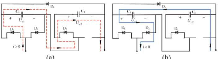
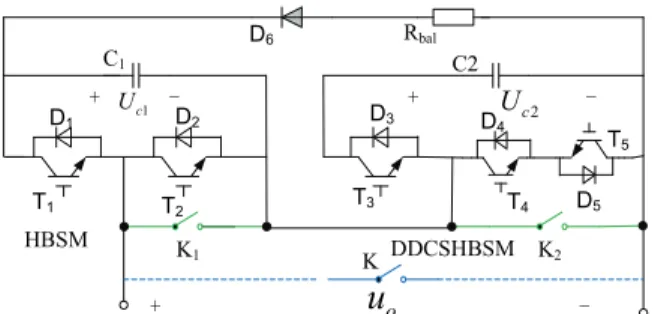
To address the overvoltage problem caused by shutdown current and to further reduce the DDCS number, HDDBSM is designed as shown in Fig. 4. Table I presents the switching function of HDDBSM. Fig. 5 shows that the bridge arm current charges the capacitor C1 after blocking and absorbs part of the energy. The fault current gradually decays to zero when the diodes are turned off.
Fig. 4 and Table I show that the zero-level output path is T2 (D2) ↔ T4 (D4) ↔ D5 (T5) or T2 (D2) ↔ T4 (T5) and that two or three power devices are present in the conduction path. Two one-level (Uc1 or Uc2) output paths are available. The first path is T1(D1) ↔C1 ↔ T4(D4) ↔ D5(T5) or T1(D1) ↔C1 ↔ T4(T5) with Uc1 output and two or three power devices.
The second path is T2(D2) ↔ T3(D3) ↔C2 or T2(D2) ↔ T3(D3) ↔C2 with Uc2 output and two power devices. The dual one-level output (Uc1+Uc2) path is T1(D1) ↔C1 ↔ T3(D3) ↔C2, which has two power devices in the conduction path.
Compared with other dual sub-modules, the clamp switch is always in the conducting state during normal operation. Therefore, the number of power devices in the conduction path stays three regardless of the output level. In sum, the power losses of HDDBSM are less than those of the dual sub-module topologies.
The cost is computed based on the number of power devices. The sub-module topology shown in Fig. 4 reveals that HDDBSM uses DDCS as a clamp switch to change the arm current path, and then the capacitor charge is realized through diode D6. Given that D6 is turned off during the MMC normal operation, the maximum voltage of D6 is
Uc1+Uc2 when the two capacitors are inserted into the arm. Therefore, this voltage is twice larger than the rated voltages of the other power devices. The arm current flows through D6 to charge the capacitors during the DC fault, and the current gradually decreases along with an increasing capacitor voltage. Therefore, the largest current occurs at the blocking moment. If the blocking time fails to meet the requirements and results in a large fault current, then the current limiting reactor can be installed on the DC link to reduce the rising rate of the fault current. As shown in Fig. 4, damping resistor Rbal can also reduce the fault current. Therefore, the maximum current of D6 is the arm current before the system blocking, and the maximum voltage is the sum of output voltages when the two sub-modules are inserted into the arm during their operation. Therefore, the D6 rated current can be selected as the other diode according to the fault current, whereas the D6 voltage can be selected as twice the rated voltage of the other IGBT.
Compared with other DC fault self-blocking sub-modules, the D6 voltage margin is same as the series sub-modules, whereas the current margin is same as the others except for the parallel sub-modules CDSM. For IGBT, the number of power devices required for each dual sub-module, such as SDSM and CDSM, is five IGBTs. However, given that the T4(D4) and T5(D5) of DDCS are connected in series as shown in Fig. 4(a), the DDCS voltage is same as the capacitor voltage UC during normal operation. Therefore, the rated voltages of T4(D4) and T5(D5) can be half of T3(D3). Given that the price of low-voltage IGBT is lower than that of high-voltage IGBT, the former may have a cost advantage. Fig. 4(b) shows that the DDCS rated voltage is similar to T3.
Bypass switches must be configured as shown in Fig. 6 to isolate them when HDDBSM is at fault. Given that HDDBSM can work independently under normal conditions similar to SM CDSM and SDSM, each SM must be configured with bypass switches K1 and K2. However, HDDBSM cannot block the DC fault when the DDCSHBSM is at fault. In 2 c U 1 c U o u 2 c U 1 c U o u bal R Rbal 1 c U Uc2 0 i 1 c U 2 c U 0 i
Fig. 6. Bypass switches configuration model of HDDBSM.
(a) (b)
Fig. 7. HDDBSM current path in the blocked model. (a) Short circuit current path. (b) Upper and lower arm equivalent circuit. addition, HBSM and DDCSHBSM must work together. Therefore, HDDBSM should be used as one SM with one bypass switch K. The SM redundancy configuration problems of self-blocking SM are studied in [20], and while the individual SM redundancy configuration is identified as the most economical choice, this configuration affects the DC fault suppression performance. Therefore, to achieve a highly economical effect, two bypass switches should be configured with HDDBSM; otherwise, only one bypass switch must be configured to achieve DC fault suppression.
III. O
PERATIONC
HARACTERISTICS OFHDDBSM-MMC
A. Analysis of the HDDBSM-MMC Inhibition Characteristic
When the pole–pole short circuit fault occurs on the DC side, phases A and B are taken as examples to illustrate the short-circuit current path in Fig. 7. The AC grid feeding and capacitors discharging currents comprise the DC side short-circuit current before blocking. The capacitors stop discharging after blocking, and the arm current gradually decreases along with an increasing arm DC voltage. The relationship between voltage and current is defined as equation (1), where R is the equivalent circuit resistance of the upper and lower arms, Rdc and Ldc are the DC circuit equivalent resistance and inductance, respectively, and N is the number of sub-modules in the upper or lower arm without considering redundant configurations (the sub-module capacitor voltage
TABLE II
COMPARISON OF DIFFERENT TOPOLOGIES
HBSM CDSM SDSM HDDBSM_1 HDDBSM_2 IGBT Diode 4 4 5 6 5 5 5 6 5 4 1+n2 0 N 2N N N λ 0 1.15 2.3 1.15 1.15 ∆ % 0 25% 25% 25%/12.5%/0% 0
is assumed to be the same as UC after blocking). During fault suppression, the inductance freewheel effect and AC voltage are overlaid together to charge the bridge arm capacitors. The inductance storage energy and AC side input power are absorbed by the capacitors and resistor. The bridge arm current decreases to zero when the AC and arm DC voltages provided by the capacitors satisfy equation (2), where Uph_m and Uline_m are the phase voltage and line voltage amplitude, respectively, m is the modulation degree, N is the number of capacitors of each arm, and Uavg is the average capacitor voltage.
(1)
(2) The fault suppression coefficient λ is defined according to equation (2) to compare the fault suppression ability of different sub-module topologies.
(3) Table II lists the fault suppression coefficients of some dual sub-module topologies with DC fault suppression capability, and ∆w is defined as the additional power loss caused by the clamp switch (where x/x/x represents the 0-, 1-, and 2-level output power losses, respectively).
B. Analysis of Capacitor Voltage Balance
When the current is negative, C2 is in the bypass state and C1 is charged as shown in Fig. 5. C1 consumes most of the circuit energy, which may excessively increase the C1 capacitor voltage and eventually lead to capacitor voltage imbalance.
Fig. 6 and the phase A arm current equation (4) both show that the inserted sub-modules in the bridge arm are in the discharging state when the converter works as a rectifier before the fault because most of the arm current is negative. By contrast, when the converter works as an inverter, most of the bridge arm current is higher than zero according to the phase A arm current equation (5), and the inserted sub- modules will be charged. Therefore, the fault current in the rectified working state is higher than that in the inverter working state after locking, and the voltage imbalance and
T3 T4 C2 D6 2 c U T1 T2 C1 1 c U -+ o
u
-+ + -T5 D1 D2 D3 D4 D5 DDCSHBSM HBSM K1 K2 K Rbal L L L L L L 1 a u a uabb 1 a i 2 b i 1 b u 2 b u 1 c u 2 c u ① ① ③ ② ② c a b c 2 a u 1 c n U a i 2 c n U 1 b i ic1 2 c i 1 a i 1 b i 2 a i 2 a i ia b i b i c i ic 2 c i 1 c n U dc i dc U dc U 2 c n U n U2 c 1 c n U
11 2
2 1 2 ab a b c a b dc dc dc dc u L di dt L di dt n n U R i i L di dt R i
_ avg _ _ avg 1 2 avg 0.5 0.5 3 0.866 ph m dc line m ph m U mU mNU U U mNU n n U
1 2
1 2
_ 1.15 30.5
c c line m c U n n U n n U mNU Novervoltage problems mainly take place in the rectified state. (4) (5) The arm energy equation can be built as equation (6), where t0 is the blocking time, and t1 is the time when the arm current decays to zero. Equation (6) shows that reducing the fault circuit energy or the energy absorbed by the capacitor C1 can partly relieve capacitor voltage imbalance problem. This goal can be achieved in three ways. First, the converter can be transformed to the inverter mode to absorb part of energy similar to traditional LCC-HVDC fault handling measures. Second, the damping resistor Rbal can be added as shown in Fig. 4. Third, the converter can be blocked as soon as possible to reduce the capacitor discharging time and the fault current. The fault current rising rate can be also limited by the reactor in the DC line.
The resistor Rbal is used to improve the capacitor voltage. Despite its benefits in absorbing power in the fault circuit, a larger resistor may lead to the transient overvoltage of the DDCS. Therefore, when selecting Rbal, the DDCS overvoltage requirement must be satisfied beforehand. The maximum Rbal can be calculated according to equation (7), where λ1 and λ2 denote the IGBT current and voltage overload coefficient, respectively, and UT and IT denote the T4 and T5 rated voltage and current, respectively.
(6)
(7)
C. Analysis of Self-startup
The traditional HBSM-MMC can take two stages of uncontrolled and fully controlled rectification to achieve system self-startup. However, for the hybrid topology, Fig. 7(a) shows that the C1 charging time is two times longer than the C2 charging time in a period. In this case, the C1 voltage becomes two times larger than the C2 voltage after the charge is completed. Moreover, given the relatively large difference between the C1 voltage Uc and rated voltage Uce, when the uncontrolled rectification stage ends, it cannot be directly transformed into a fully controlled rectification. To easily describe the charging degree, the charging rate (CR) is defined as equation (8), where M is the number of charging capacitors in the charging circuit.
(8)
For the HBSM topology (M=N), the theoretical charging rate CRHBSM is defined as equation (9), and the difference between capacitor voltages Uc and Uce is small.
(9) For the hybrid topology, the capacitor charging rate of the sub-module differs from the rated voltage and is defined by equations (10) and (11). Because the HBSM voltage can reach half of the rated value after uncontrolled rectification, the control unit can be powered by these capacitors, it can bypass HBSM using control logic to complete the auxiliary charge and reduce the voltage deviation when uncontrolled rectification stage ends.
(10) (11) By taking the lower bridge arm as example, the lower phase bridge arm sub-modules are divided into {(A_HBSM A_DDCSHBSM) (B_HBSM B_DDCSHBSM ) (C_HBSM C_DDCSHBSM)} according to their topologies. When the uncontrolled rectification stops charging, the lower bridge arms A_HBSM, B_HBSM, and C_HBSM are bypassed, and the number of charging sub-modules in the charging circuit is reduced to N. The uncontrolled rectification state is then used to charge the bridge arm sub-module capacitors. The charging state is consistent with the traditional half-bridge topology. When the capacitor voltage in the charging circuit reaches the half-bridge topology limit, the voltage charging rate △CR is defined as equation (12). The system then reduces the difference between the rated voltages and can be transformed to a full-controlled rectification to charge all sub-module capacitors to the rated voltage.
(12)
(13)
IV. R
ESULTSA. Study System
To verify the fault suppression ability of the improved topology, the MMC-HVDC simulation model shown in Fig. 8 is applied in PSCAD/EMTDC. The system parameters are shown in Table III.
B. Analysis of Self-startup
According to equations (10) and (11), the hybrid topology capacitor voltage in the first stage can be calculated as 0.577*20=11.5 kV and 0.288*20=5.76 kV, respectively, whereas according to equations (12) and (13), the voltage in
1 3 3 0.5 sin
a dc a dc m i i i i I t
1 3 3 0.5 sin
a dc a dc m i i i i I t
2 2 2 2 1 2 1 2 1 2 1 2 0 2 2 2 1 2 1 0 1 0 ( ) 2 2 2 ( ) 2 a b t dc dc c ab a t t c a b dc dc t L i i L i n n CU t u i dt n n CU t R i i R i dt
_ max 1 2 bal T c T R I U U
_ _
2 3 2 2 2 3 line m c ce line m U M U mN CR U U mN M HBSM 23mN 32m 0.866 CR M HBSM0.866 2 2 1 ( ) 0.577 CR DDCSHBSM0.866 1 (2 1) 0.288 CR
HBSM DDCSHBSM
0.866 0.5 1 2 1 1 0.866 1 0.288 3 2 3 CR CR CR N N HBSM DDCSHBSM 0.577 0.288 0.865 0.288 0.288 0.576 CR CR Fig. 8. Two-terminal model of the simulation. TABLE III MAIN CIRCUIT PARAMETERS
Items Value
Rated DC voltage +/-200kV
Rated active power 400MW
AC system source voltage 210kV
AC system source frequency 50Hz
Transformer ratio 210 kV/220 kV Y0/ D Transformer leakage inductance 0.1pu
Number of SM per arm 20
SM capacitance C0 3000uF
Arm inductance L0 0.1pu
SM capacitor voltage 20kV
(a)
(b)
(c)
Fig. 9. Self-startup of HDDBSM-MMC. (a) Lower bridge arm capacitance voltage in phase A. (b) AC current. (c) DC bus voltage.
(a)
(b)
(c)
Fig. 10. Comparison of the DC link fault blocking effect. (a) Phase A bridge current. (b) Phase A AC current. (c) DC current. the second stage can be computed as 0.865*20 =17.3 kV and 0.576*20=11.5 kV, respectively. Fig. 9 shows that the capacitor voltage reaches 6 kV and 12 kV after the first uncontrolled rectification stage, whereas the sub module capacitor voltage stabilizes at 12 kV and 17 kV after the auxiliary charging of the bypass HBSM. These results are consistent with those of the theoretical analysis.
In the fully controlled rectification charging mode, all sub-module capacitors are charged to the rated voltage of 20 kV. The converter DC bus voltage is shown in Fig. 9(c).
C. Comparison of Fault Suppression Characteristics
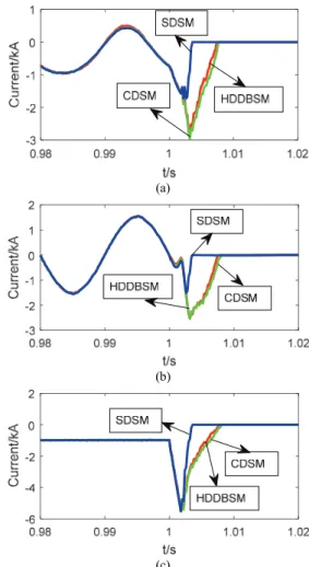
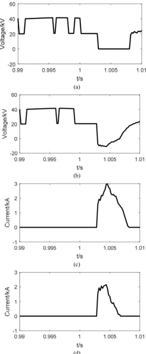
Fig. 10 presents the simulation results for the DC-side fault suppression effects of the SDSM, HDDBSM, and CDSM topologies. When the bridge arm current is negative after blocking, the two capacitors of SDSM are in a series charging state and have a maximum output voltage of Uc1+Uc2, the two capacitors of CDSM are in a parallel charging state and have a maximum output voltage of Uc1//Uc2, and only one capacitor of HDDBSM is charged and has an output voltage of Uc1. Therefore, compared with CDSM and HDDBSM, SDSM has a larger DC fault suppression coefficient and a shorter time of fault current decaying to zero. While the
(a) (b)
(c) (d)
Fig. 11 DC link fault unblocking effect. (a) DC link voltage. (b) DC link current. (c) AC current. (d) Upper and lower arm voltages of phase A.
(a) (b)
Fig. 12. DC link fault blocking feature comparison. (a) Phase A bridge arm inductance voltage. (b) DC current. number of capacitors in the blocking state and the theoretical
fault suppression coefficients of CDSM and HDDBSM are the same, the HBSM capacitor voltage is higher than the CDSM capacitor voltage due to parallel charging. In Figs. 10(a) to 10(c), some differences can be observed in the time required for the current to decay to zero. In sum, SDSM shows the best fault suppression ability, and very small differences can be found in the fault suppression abilities of CDSM and HDDBSM.
D. Unblocking Fault Suppression Characteristics
Although the direct and simple fault suppressing method for HDDBSM is to block system as CDSM and SDSM, longer blocking system may cause capacitor voltages to divergence and the AC breaker will be triggered to cut off fault current, this may result in longer system recovery time . According to Table I, the HDDBSM can output a negative voltage when the bridge arm current is negative, while the HDDBSM positive voltage output is not constrained by the current direction of the bridge arm. When the bridge arm current is positive, the sub-module capacitor is charged in
series when inserted, which can block the bridge arm current as illustrated in Fig. 7(b). Therefore, how to suppress the negative bridge arm current must be examined. According to the current direction illustrated in Fig. 7(b), the upper arm current is blocked naturally in phase B, ub1>0, while the lower arm can output the negative voltage ub2<0. Following the full bridge sub-module topology DC fault suppression proposed in [5], [6], this paper uses HDDBSM negative level output characteristics to control the DC voltage to zero and to suppress the lower arm fault current.
Fig. 11 shows that the upper- and lower-arm voltages have opposite polarity characteristics. In this case, the DC voltage during fault is approximately zero, thereby preventing the converter from being blocked. After the fault is over, the system, the AC and DC currents, and the voltages all return to normal.
E. Analysis of Capacitor Voltage Balance
DDCSHBSM does not face the capacitor voltage unbalance problem. However, Fig. 12(a) shows that because the bridge arm is cut off instantly, the bridge arm inductance induces a
1 1.5 2 2.5 -200 0 200 400 600 t/s V ot age/ kV 1 1.5 2 2.5 -2 0 2 4 6 t/s C urrent /k A 1 1.5 2 2.5 -2 -1 0 1 2 t/s C ur re nt/k A 1 1.1 1.2 1.3 1.4 t/s -400 -200 0 200 400 0.99 0.995 1 1.005 1.01 t/s -10 -5 0 5 HDDBSM DDCSHBSM
(a)
(b)
(c)
Fig. 13. Effect of blocking time and balancing resistor on upper bridge arm capacitance voltage in phase A with (a) t=0.002 s and
Rbal=0, (b) Rbal=0, and t=0.001 s, and (c) Rbal=5Ω and t=0.002 s.
large voltage. Although the number of charging capacitors in the path is 2N, which is greater than the valve side AC line voltage amplitude, the current should theoretically become zero, but the large inductive and AC voltages work together to conduct the diode again. The DC current waveform is shown in Fig. 12(b). For HDDBSM, the bridge inductance does not produce a large inductive voltage, and the DC current does not reverse as it avoids the current from being cut off immediately.
Fig. 13 shows the influences of blocking time and balancing resistor on the two capacitor voltages in the HDDBSM topology. In this figure, λ1=λ2=2, UT1≈UC =20 kV, DC current
Idc=1 kA, AC current amplitude Iac_m=1.5 kA, Rbal can be calculated using equation (14), and half of the maximum Rbal is chosen in the simulation.
(14) Figs. 13(a) and (b) show that the improvement in the fault detection measures and rapid blocking system can effectively
(a)
(b)
(c)
(d)
Fig. 14. Voltage and current of D6 with different Rbal. (a) Voltage with Rbal=0. (b) Voltage with Rbal=5Ω. (c) Current with Rbal=0. (d) Current with Rbal=5Ω.
alleviate the capacitor voltage imbalance. Figs. 13(a) and (c) also reveal that the voltage across the HBSM capacitor C1 in the hybrid topology is high when the converter operates in a rectifying state without a balance resistor, while Rbal can reduce the voltage difference between C1 and C2.
Figs. 14(a) and (b) show that the voltage of D6 stays at 40 kV when HDDBSM outputs Uc1+Uc2 or when HBSM is bypassed and DDCSHBSM is inserted, while its voltage is only 20 kV when DDCSHBSM is bypassed and HBSM is inserted. Moreover, Rbal shows only a slight effect on voltage. The current of D6 before blocking is zero because the diode is
2 1 C _ max 1 1 _ 20 9.23 2 3 2 T bal T dc ac m U U R I I Ireverse biased, the arm current flowing through D6 after blocking mainly depends on the magnitude of the fault current, and a large fault current can be limited to a lower level by Rbal as shown in Figs. 14(c) and (d).
V. C
ONCLUSIONSTo suppress the DC short circuit fault current in MMC- HVDC, this paper summarizes the fault suppression characteristics of three sub-modules with a DC fault blocking ability. To reduce the number of devices that consume a large amount of energy in the existing sub-module topologies, this paper designs DDCSHBSM to realize DC fault blocking and proposes the hybrid sub-module topology HDDBSM to overcome the shortcomings of DDCSHBSM. According to the number of sub-modules in the bridge arm charging circuit, the fault suppression characteristics and self-startup strategy of the DC transmission system with HDDBSM topology are examined. This study is conducted in the time domain by using the PSCAD/EMTDC simulation environment. The simulation results verify the effectiveness of the hybrid topology and control strategy for DC side fault suppression.
A
CKNOWLEDGMENTThis work was supported by the Hebei Natural Science Foundation of China under Grant No. E2019502123.
R
EFERENCES[1] R. Marquardt, “Modular multilevel converter topologies with dc-short circuit current limitation,” in Proc. of IEEE
8th Int. Power Electron. ECCE Asia Conf, pp1425-1431,
2011.
[2] J. Qin, M. Saeedifard, A. Rockhill, and R. Zhou, “Hybrid design of modular multilevel converters for HVDC systems based on various sub module circuits,” IEEE Trans. Power
Del., Vol. 30, No. 1, pp. 385-394, Feb. 2015.
[3] J. Zhang and C. Zhao, “The research of SM topology with DC fault tolerance in MMC-HVDC,” IEEE Trans. Power
Del., Vol. 30, No. 3, pp. 1561-1568, Jun. 2015.
[4] R. Zeng, L. Xu, L. Yao, and B. W. Williams, “Design and operation of a hybrid modular multilevel converter,” IEEE
Trans. Power Electron., Vol. 30, No. 3, pp. 1137-1146,
Mar. 2015.
[5] J.-J. Jung, S. Cui, J.-H. Lee, and S.-K. Sul, “A new topology of multilevel VSC converter for a hybrid HVDC transmission system,” IEEE Trans. Power Electron., Vol. 32, No. 6, pp.4199-4211, Jun. 2017.
[6] W. Lin, D. Jovcic, S. Nguefeu, and H. Saad, “Full-bridge MMC converter optimal design to HVDC operational requirements,” IEEE Trans. Power Del., Vol. 31, No. 3, pp. 1342-1350, Jun. 2016.
[7] T. H. Nguyen and D. C. Lee, “Protection of the MMCs of HVDC transmission systems against DC short-circuit
faults,” J. Power Electron., Vol. 17, No. 1, pp. 232-241, Jan. 2017.
[8] X. Yu, Y. Wei, Q. Jiang, X. Xie, Y. Liu, and K. Wang, “A novel hybrid-arm bipolar MMC topology with DC fault ride through capability,” IEEE Trans. Power Del., Vol. 32, No. 3, pp. 1404-1413, Jun. 2017.
[9] R. Li, G. P. Adam, D. Holliday, J. E. Fletcher, and B. W. Williams, “Hybrid cascaded modular multilevel converter with DC fault ride-through capability for the HVDC transmission system,” IEEE Trans. Power Del., Vol. 30, No. 4, pp. 1853-1862, Aug. 2015.
[10] R. Li, J. E. Fletcher, L. Xu, D. Holliday, and B. W. Williams, “A hybrid modular multilevel converter with novel three level cells for DC fault blocking capability,”
IEEE Trans. Power Del., Vol. 30, No. 4, pp. 2017-2026,
Aug. 2015.
[11] A. Elserougi, A. M. Massoud, and S. Ahmed, “A switched-capacitor sub module for modular multilevel HVDC converters with DC-fault blocking capability and a reduced number of sensors,” IEEE Trans. Power Del., Vol. 31, No. 1, pp. 313-322, Feb. 2016.
[12] A. Nami, L. Wang, and F. Dijkhuizen. “Five level cross connected cell for cascaded converters,” European Power
Electronics and Applications Conference (EPE), 2013.
[13] A. Nami, J. Liang, F. Dijkhuizen, and G. D. Demetriades, “Modular Multilevel Converters for HVDC applications: Review on converter cells and functionalities,” IEEE Trans.
Power Electron., Vol. 30, No. 1, pp. 18-36, Jan. 2015.
[14] X. Li, Q. Song, W. Liu, H. Rao, S. Xu, L. Li, “Protection of nonpermanent faults on DC overhead lines in MMC-Based HVDC system,” IEEE Trans. Power Del., Vol. 28, No. 1, pp. 483-490, Jan. 2013.
[15] Petar J. Grbovic, F. Gruson, N. Idir, and P. Le Moigne, “Turn-on performance of reverse blocking IGBT (RB IGBT) and optimization using advanced gate driver,” IEEE
Trans. Power Electron., Vol. 25, No. 4, pp. 970-981, Apr.
2010.
[16] C. Klumpner, P. Nielsen, I. Boldea, and Frede Blaabjerg, “New solutionsfor a low-cost power electronic building block for matrix converters,” IEEE Trans. Ind. Electron., Vol. 49, No. 2, pp. 336-344, Apr. 2002.
[17] J. Itoh, I. Sato, A. Odaka, H. Ohguchi, H. Kodachi, and N. Eguchi, “Anovel approach to practical matrix converter motor drive system with reverse blocking IGBT,” IEEE
Trans. Power Electron., Vol. 20, No. 6, pp. 1356-1363,
Nov. 2005.
[18] C. Klumpner and F. Blaabjerg, “Using reverse-blocking IGBTs in power converters for adjustable-speed drives,”
IEEE Trans. Ind. Appl., Vol. 42, No. 3, pp. 807-816, May/
Jun. 2006.
[19] M. Callavik, A. Blomberg, J. Hafner, and B. Jacobson, “The hybrid HVDC breaker - An innovation breakthrough enabling reliable HVDC grids,” ABB Grid Systems, Technical paper, 2012.
[20] J. Xu, P. Zhao, and C. Zhao, “Reliability analysis and redundancy configuration of MMC with hybrid sub-module topologies,” IEEE Trans. Power Electron., Vol. 31, No. 4, pp. 2721-2732, Aug. 2016.
Jianpo Zhang was born in Hebei Province,
China. He received his M.S. degree from Tianjing University in 2005 and his Ph.D. degree from North China Electric Power University in 2013. He is currently working as a teacher in North China Electric Power University. His main research interests include the application of VSC–HVDC and flexible AC transmission systems.
Diqiong Cui was born in Hebei Province,
China. He received his B.S. degree from Hebei University in 2019, and he is currently pursuing his M.S. degree in electrical engineering in North China Electric Power University. His research interests include the application of VSC–HVDC and flexible AC transmission systems.
Xincheng Tian was born in Hebei Province,
China. He received his M.S. degree from North China Electric Power University in 2002, and he is currently working as a senior engineer in the Tangshan Power Corporation of China State Grid. His research interests include the application of VSC–HVDC and power scheduling automation.
Chengyong Zhao was born in Zhejiang
Province, China. He received his B.S., M.S., and Ph.D. degrees in power system and its automation from North China Electrical Power University, Beijing, China, in 1988, 1993, and 2001, respectively. He is currently serving as the deputy director of the New Energy Power Grid Institute in the Electrical and Electronic Engineering School, North China Electric Power University, Beijing, China. His research interests include HVDC, flexible AC transmission systems, and power quality.