Surface-normal electro-optic spatial light
modulator using graphene integrated on a
high-contrast grating resonator
T
IANBOS
UN,
1,6J
ONGHWANK
IM,
2,6J
ONGM
INY
UK,
2,3,4,5A
LEXZ
ETTL,
2,3,4F
ENGW
ANG,
2,7ANDC
ONNIEC
HANG-
HASNAIN1,81EECS Department, University of California at Berkeley, Berkeley, CA 94720, USA 2Physics Department, University of California at Berkeley, Berkeley, CA 94720, USA
3Materials Sciences Division, Lawrence Berkeley National Laboratory, Berkeley, CA 94720, USA 4Kavli Energy NanoScience Institute at the Univeristy of California, Berkeley and the Lawrence
Berkeley National Laboratory, Berkeley, CA 94720, USA
5Department of Materials Science and Engineering, Korea Advanced Institute of Science and
Technology (KAIST), Daejeon 305-701, South Korea
6These authors contributed equally to this work 7fengwang76@berkeley.edu
8cch@berkeley.edu
Abstract: We demonstrate efficient optical modulation of surface-normal reflection in a
novel device structure integrating graphene on a high contrast grating (HCG) resonator. As high as 11 dB extinction ratio is achieved by varying the voltage applied to a single atomic layer of graphene on a HCG resonator. The device topology facilitates easy fabrication of large 2D arrays, and free-space operation. We also demonstrate a graphene-oxide-graphene structure which can potentially operate at MHz operation speed. The devices are fully fabricated by standard CMOS compatible processes indicating that the integrated structure of graphene-on-HCG shows great promise for display, imaging and interconnects applications with low-cost and large scalability.
© 2016 Optical Society of America
OCIS codes: (140.4780) Optical resonators; (130.0130) Integrated optics.
References and links
1. G. T. Reed, G. Mashanovich, F. Y. Gardes, and D. J. Thomson, “Silicon optical modulator,” Nat. Photonics 4(8), 518–526 (2010).
2. J. A. Neff, R. A. Athale, and S. H. Lee, “Two-dimensional spatial light modulator: a tutorial,” Proc. IEEE 78(5), 826–855 (1990).
3. B.-W. Yoo, M. Megens, T. Chan, T. Sun, W. Yang, C. J. Chang-Hasnain, D. A. Horsley, and M. C. Wu, “Optical phased array using high contrast gratings for two dimensional beamforming and beamsteering,” Opt. Express 21(10), 12238–12248 (2013).
4. F. Bonaccorso, Z. Sun, T. Hasan, and A. C. Ferrari, “Graphene photonics and optoelectronics,” Nat. Photonics
4(9), 611–622 (2010).
5. Z. Sun, A. Martinez, and F. Wang, “Optical modulators with 2D layered materials,” Nat. Photonics 10(4), 227– 238 (2016).
6. R. R. Nair, P. Blake, A. N. Grigorenko, K. S. Novoselov, T. J. Booth, T. Stauber, N. M. R. Peres, and A. K. Geim, “Fine structure constant defines visual transparency of graphene,” Science 320(5881), 1308 (2008). 7. K. F. Mak, M. Y. Sfeir, Y. Wu, C. H. Lui, J. A. Misewich, and T. F. Heinz, “Measurement of the optical
conductivity of graphene,” Phys. Rev. Lett. 101(19), 196405 (2008).
8. F. Wang, Y. Zhang, C. Tian, C. Girit, A. Zettl, M. Crommie, and Y. R. Shen, “Gate-variable optical transitions in graphene,” Science 320(5873), 206–209 (2008).
9. Z. Q. Li, E. A. Henriksen, Z. Jiang, Z. Hao, M. C. Martin, P. Kim, H. L. Stormer, and D. N. Basov, “Dirac charge dynamics in graphene by infrared spectroscopy,” Nat. Phys. 4(7), 532–535 (2008).
10. Y. Lee, S. Bae, H. Jang, S. Jang, S.-E. Zhu, S. H. Sim, Y. I. Song, B. H. Hong, and J.-H. Ahn, “Wafer-scale synthesis and transfer of graphene films,” Nano Lett. 10(2), 490–493 (2010).
11. Y.-M. Lin, A. Valdes-Garcia, S.-J. Han, D. B. Farmer, I. Meric, Y. Sun, Y. Wu, C. Dimitrakopoulos, A. Grill, P. Avouris, and K. A. Jenkins, “Wafer-scale graphene integrated circuit,” Science 332(6035), 1294–1297 (2011). 12. J. Kim, H. Son, D. J. Cho, B. Geng, W. Regan, S. Shi, K. Kim, A. Zettl, Y.-R. Shen, and F. Wang, “Electrical
control of optical plasmon resonance with graphene,” Nano Lett. 12(11), 5598–5602 (2012).
#275113 http://dx.doi.org/10.1364/OE.24.026035
13. A. Majumdar, J. Kim, J. Vuckovic, and F. Wang, “Electrical control of silicon photonic crystal cavity by graphene,” Nano Lett. 13(2), 515–518 (2013).
14. Y. Gao, R.-J. Shiue, X. Gan, L. Li, C. Peng, I. Meric, L. Wang, A. Szep, D. Walker, Jr., J. Hone, and D. Englund, “High-speed electro-optic modulator integrated with graphene-boron nitride heterostructure and photonic crystal nanocavity,” Nano Lett. 15(3), 2001–2005 (2015).
15. C. T. Phare, Y.-H. Daniel Lee, J. Cardenas, and M. Lipson, “Graphene electro-optic modulator with 30 GHz bandwidth,” Nat. Photonics 9(8), 511–514 (2015).
16. M. Liu, X. Yin, E. Ulin-Avila, B. Geng, T. Zentgraf, L. Ju, F. Wang, and X. Zhang, “A graphene-based broadband optical modulator,” Nature 474(7349), 64–67 (2011).
17. C. Qiu, W. Gao, R. Vajtai, P. M. Ajayan, J. Kono, and Q. Xu, “Efficient modulation of 1.55 μm radiation with gated graphene on a silicon microring resonator,” Nano Lett. 14(12), 6811–6815 (2014).
18. Y. Yao, M. A. Kats, P. Genevet, N. Yu, Y. Song, J. Kong, and F. Capasso, “Broad electrical tuning of graphene-loaded plasmonic antennas,” Nano Lett. 13(3), 1257–1264 (2013).
19. S. Junique, Q. Wang, S. Almqvist, J. Guo, H. Martijn, B. Noharet, and J. Y. Andersson, “GaAs-based multiple-quantum-well spatial light modulators fabricated by a wafer-scale process,” Appl. Opt. 44(9), 1635–1641 (2005). 20. C. J. Chang-Hasnain and W. Yang, “High-contrast gratins for integrated optoelectronics,” Adv. Opt. Photonics
4(3), 379–440 (2012).
21. T. Sun, W. Yang, and C. Chang-Hasnain, “Surface-normal coupled four-wave mixing in a high contrast gratings resonator,” Opt. Express 23(23), 29565–29572 (2015).
22. T. Sun, S. Kan, G. Marriott, and C. Chang-Hasnain, “High-contrast grating resonators for label-free detection of disease biomarkers,” Sci. Rep. 6, 27482 (2016).
23. K. S. Kim, Y. Zhao, H. Jang, S. Y. Lee, J. M. Kim, K. S. Kim, J.-H. Ahn, P. Kim, J.-Y. Choi, and B. H. Hong, “Large-scale pattern growth of graphene films for stretchable transparent electrodes,” Nature 457(7230), 706– 710 (2009).
24. X. Li, W. Cai, J. An, S. Kim, J. Nah, D. Yang, R. Piner, A. Velamakanni, I. Jung, E. Tutuc, S. K. Banerjee, L. Colombo, and R. S. Ruoff, “Large-area synthesis of high-quality and uniform graphene films on copper foils,” Science 324(5932), 1312–1314 (2009).
25. M. Liu, X. Yin, and X. Zhang, “Double-layer graphene optical modulator,” Nano Lett. 12(3), 1482–1485 (2012). 26. B. Sukang and K. Hyeong, X. XianFang, B. Jayakumar, L. Tian, S. Youngil, K. Young Jin, O. Barbaros, A.
Jong-Hyun, H. Byung Hee, and I. Sumio, “30-inch roll-based production of high-quality graphene films for flexible transparent electrodes,” in CORD Conference Proceedings (2009).
1. Introduction
Electro-optic (EO) modulation is an essential operation in photonic and optoelectronic application ranging from optical interconnect to bio/chemical sensing and imaging [1–3]. Recently, graphene has emerged as a novel optical medium for EO modulators owing to its unique optoelectronic properties. Graphene, as a zero band gap semiconductor, absorbs light in the extremely broad spectral range from terahertz to ultraviolet frequency [4–7]. Remarkably, electrostatic gating of graphene can efficiently tune this broadband light absorption [8, 9]. Such excellent gate-tunability in light absorption is particularly attractive for the EO applications at optical frequencies from visible to telecom frequencies where conventional semiconductors exhibit limited tunability. Furthermore, it has been shown that graphene can be grown in the large scale and readily combined with CMOS process [10, 11].
The most critical challenge for graphene toward practical applications, however, lies in its small light absorption. A single atomic thickness of graphene significantly limits the total light absorption to ~2.3% upon surface normal incidence [6–8], although its absorption coefficient is actually an order of magnitude larger than the band edge absorption of a typical direct bandgap semiconductor, e.g. GaAs. Integration of graphene with photonic structures has demonstrated that light absorption can be greatly enhanced via enhancing interaction cross-section from waveguide mode or amplifying electric field from strong cavity resonance. Various engineered structures have been explored including Si waveguides, photonic crystal cavities or ring resonators [5, 12–18]. However, these structures do not facilitate the fabrication of 2D arrays, and free-space operation for 3D free-space based applications such as imaging, display, holographic and remote sensing. Extending the dimension from a planar optical circuit into a 3D free-space system can significantly expand the capability and scalability of optical system in the aforementioned applications.
Here, we demonstrate a new free-space graphene-based spatial light modulator (SLM) with the use of a novel surface-normal high contrast grating (HCG) resonator. High contrast
grating (HCG) is a single ultrathin layer of near-wavelength gratings fully surrounded by media having a large contrast in refractive indices. It exhibits many distinct features nonexistent in conventional gratings [20]. In particular, it can be designed to exhibit a very high quality factor resonance for optical beam incident in the surface-normal direction with a high coupling efficiency via free-space excitation [21, 22]. These attributes are ideal for integrating with graphene for EO modulator in 3D free-space applications. Integrated structure of graphene and HCG is realized via a CMOS-compatible process, including standard optical lithography and graphene transfer techniques, eliminating the inefficiency and high-cost of e-beam lithography which is commonly used for graphene modulators in the previous reports. Reflection spectroscopy shows that optical resonances in HCG can be efficiently tuned with a maximum modulation depth of 11 dB by electrostatic gating of graphene, which is substantially superior to other EO spatial light modulator scheme based on GaAs quantum wells both in modulation depth and CMOS compatibility [19]. Free space coupling scheme with large modulation depth and simple fabrication process of our architecture facilitates the fabrication of large 2D array which is extremely promising for applications in optical imaging, telecommunication, bio/chemical sensing at optical frequencies.
2. Optical Resonance in HCG for Efficient Free-space Coupling with Graphene
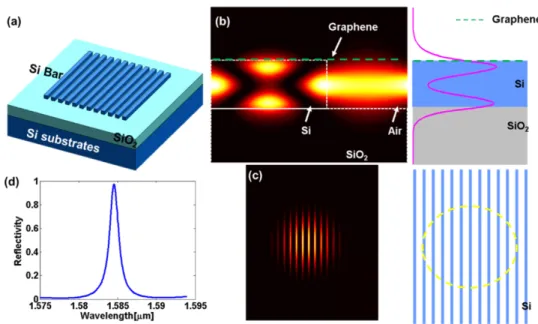
A high-Q HCG resonator for surface-normal incident beam is formed on an ultra-thin layer (< 200 nm) of silicon on insulator (SOI) substrate, schematically shown in Fig. 1(a). Silicon gratings with near-wavelength dimensions, fully surrounded by materials with low refractive indices, i.e. air and silicon dioxide, form this unique resonator. The basic principle of HCG works as follows. By choosing appropriate grating period and duty cycle, a HCG design supporting only two grating modes can be easily obtained. Leveraging the high contrast in refractive indices at both the entrance and exit planes, a strong coupling is achieved between the intrinsic grating modes at the boundaries. With the right thickness, these two grating modes can be made to interfere constructively at the entrance and exit boundaries, resulting in a high-Q resonator with light propagating in the direction normal to the grating plane. This unique phenomenon was analyzed and reported previously [20–22]. A detailed quantitative analysis of the design algorithm employed for the HGG resonator is described in Sections 1 & 4 of reference 20.
The cavity resonance of HCG has two outstanding advantages for enhancing light modulation with graphene upon free space coupling. First of all, the cavity mode exhibits excellent spatial overlap with graphene on the grating surface, which is essential for the light absorption in graphene. Figures 1(b) and 1(c) show intensity profile of in-plane electric field for the cavity resonance under a collimated Gaussian beam (10 um size) at normal incidence. In the vertical direction (Fig. 1(b)), a large portion of the resonance mode is exposed on the HCG surface where graphene can be readily transferred (green dashed line). In comparison, a simple Fabry-Perot cavity does not have strong electric field at the surface, leading to weak light absorption in graphene. Figure 1(c) shows the top view of the resonance sliced in the center of the grating slab. The mode profile in the horizontal direction is only limited by incident Gaussian beam (yellow dashed line in the schematic), which can cover large area of graphene on the surface. Secondly, total reflection from HCG in the free space is completely dominated by the cavity resonance. Figure 1(d) shows a simulated optical reflection spectrum where free space reflectivity exhibits nearly 100% at the optical resonance. Therefore, remarkably large modulation depth can be achieved in the free space reflection efficiently via controlling the cavity resonance with light absorption in graphene.
Fig. 1. (a) Schematic of HCG. (b) Side view of simulated optical mode inside one period of HCG resonator. (c) Top view of HCG resonator under excitation of 10um Gaussian beam. (d) Simulated reflection spectrum for HCG resonator
3. Device Demonstration and Optical Characterization
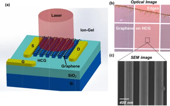
Figure 2(a) schematically illustrates the device structure for the experimental demonstration. HCG are patterned onto a 6 inch silicon-on-insulator wafer using deep ultraviolet (DUV) lithography, followed by silicon refractive ion etching, both standard processes in semiconductor manufacturing. For HCG devices used in this study, the grating period is 792 nm, the barwidth is 427 nm, and grating thickness is 500 nm. On top of the HCG resonator, we transferred a large-area (~3cm x 3cm) graphene grown by chemical vapor deposition using the standard growth and transfer processes [23, 24]. Figures 2(b) and 2(c) show representative optical microscope and scanning electron microscope (SEM) images of the hybrid graphene-Si HCG structure, respectively. Both microscope images show that monolayer graphene is successfully transferred on the HCG surface. For electrostatic gating, we use Au-graphene contact to form source, drain and a top electrolyte gating with ion-gel. Optical cavity resonance is characterized via reflection spectroscopy. A supercontinuum laser as a broadband light source is illuminated in surface-normal direction as shown in Fig. 2(a) where incident light is linearly polarized, parallel to the HCG plane and the high contrast grating is aligned at 45 degree with the input light polarization. We collect cross polarized reflected light which is analyzed by a spectrometer equipped with an InGaAs array detector.
Fig. 2 on top Figure 3(a Bare HCG (re of ~1000. Rem curve). Cavity resonator. Th electromagnet interband opti Fig. 3 of gat eV). 4. Electrost In order to mo electrolyte. A 2. (a) Schematic of p of HCG. (c) SEM a) shows reflec ed curve) show markably, a sin y reflected po is strong damp tic coupling b ical transition i
3. (a) Cavity reflec te-tunable interban
atic Modulat
odulate cavity At low drive vol
f HCG graphene s M of HCG structur ction spectra of ws a prominent ngle atomic-lay wer decrease ping of the reso by which elec in graphene.
ction (power) befo nd transition in gr
tion of HCG C
reflectivity, we ltage, HCG cav
spatial light modul re with mono-layer f bare HCG an cavity resonan yer graphene re by ~14 dB at onance is owin ctromagnetic f
ore and after graph raphene at cavity r
Cavity Reson
e gate the grap vity reflection
lator. (b) Optical i r graphene on top.
nd the hybrid s nce at 1572 nm
enders the cav resonance wa ng to light abs field in the c hene transfer. (b) a resonance frequen nance with G phene by mean is rendered to image of graphene . structure with g m with the qual vity nearly opaq
avelength of b orption in grap avity is dissip and (c) Illustration ncy wR ( = 0.86 Graphene ns of the ion-ge be an ‘off’ stat e graphene. lity factor que (Blue bare HCG phene via pated via n 6 el as a top te. As the
voltage is tuned to gate graphene hole-doping side, HCG cavity reflection is rendering to be an ‘on’ state. We observe significant narrowing in the cavity line width as well as dramatic increase in the cavity reflectivity. This switching can be qualitatively understood by simple illustration in Figs. 3(b) and 3(c). For charge neutral case (Fig. 3(b)), Fermi level is located at Dirac point and interband transition exhibits strong light absorption in graphene at the cavity resonance energy, wR. However, this strong interband transition can be turned off by shifting Fermi level below half of the cavity resonance energy 1/2 wR via electrostatic doping as shown in Fig. 3(c): the optical transition is forbidden via Pauli blocking since initial electronic state is unoccupied. Alternatively, interband transition can be also turned off via Pauli blocking by shifting Fermi level above 1/2 wR in which case final electronic state is occupied.
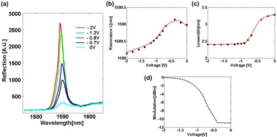
Figure 4 shows the effect of the electric field on the graphene-HCG device. We measure the cavity reflection spectrum while varying the gate voltage from 0 V to −2 V where Fermi level of graphene is tuned from charge neutral case to hole-doped case. Black dots in Figs. 4(b)-4(d) summarize electrostatic gate modulation of the cavity resonance in terms of resonance wavelength, linewidth and reflectivity, respectively. Observed cavity resonance energy shift and linewidth can be attributed to the change in complex dielectric constant of graphene, which is reported in the theory section of reference 9. To conclusively prove that the change in resonance are due to graphene, we theoretically fit our experimental observations following the model in our previous work (Red curves). Excellent agreement between experiment and theoretical predication indicates that cavity modulation is dominated by graphene absorption. In terms of cavity reflectivity, an 11dB modulation depth is achieved within 2V voltage swing shown clearly in Fig. 4(d). Modulation saturates at around −2V, at which interband transition at resonance wavelength is blocked and graphene is transparent.
Fig. 4. (a) Cavity reflectivity for gating voltage from −2V to 0V. (b) Resonance wavelength as function of gate voltage. Red curve shows theoretical fitting. (c) Resonance linewidth as function of applied voltage. Red curve shows theoretical fitting. (d) Cavity peak reflection as function of applied voltage. An 11dB modulation is achieved within 2V voltage swing.
5. Towards Large Scale Fast Spatial Light Modulator
In the previous section, we have used ion-gel to electrostatically dope graphene to demonstrate the capability to modulate the HCG resonance by gating graphene. To show the high speed operation potential of our proposed modulator, we employ the graphene-oxide-graphene structure integrated with HCG, in which two layers of graphene-oxide-graphene are separated by
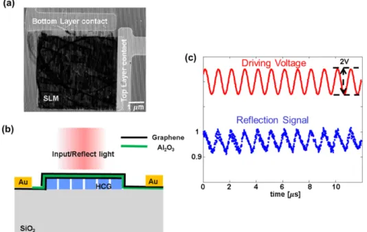
Al2O3 grown by ALD (Cambridge) and integrated on top of HCG cavities. Both electron and holes are injected into graphene layers. When the driving voltage is close to zero, both graphene layers are undoped. Therefore, Fermi levels are close to the Dirac point, and both graphene sheets are light absorptive. Consequently, cavity transmission is low and modulation state is ‘off’. When a voltage is applied across graphene-oxide-graphene structure, two graphene layer form a parallel capacitor with two graphene layer doped by holes and electrons separately by the same carrier concentration. When the Fermi level shift in both graphene layers reach more than half of the cavity resonance energy, both graphene layers become transparent simultaneously. In this case, cavity transmission will be high and modulation state is ‘on’ [25]. An SEM image of a fabricated graphene-oxide-graphene HCG modulator with top and bottom contact is shown in Fig. 5(a). Device fabrication process is similar to the method described in reference [25], including HCG definition, bottom graphene layer transfer and definition, bottom contact, ALD, top layer graphene transfer and definition, and top layer contact. The whole fabrication is based on photolithography and Si compatible process. Schematic from side view of final structure is shown in Fig. 5(b).
To demonstrate the high speed operation, sinusoidal driving voltage with 1 MHz frequency (shown as red curve in Fig. 5(c)) is applied across top and bottom graphene. Reflection signal is collected and shown in the blue curve in Fig. 5(c). Speed measurement in the experiment is limited by the poor electrical contact between Au and graphene and with process improvement, we expect higher operation speed. In theory, a 20um x 20um graphene-oxide-graphene structure has capacitance around 6.8 pf (assuming 5nm ALD layer). Resistance for the device can be as low as 30 Ω / sq with moderately doped graphene [13, 26]. These lead to 0.78GHz operation speed theoretically. Only 9% modulation depth is shown in this measurement, due to graphene damage in the transfer process (shown in the SEM) and oversized illumination of the incident beam, which can be improved with optimized fabrication process and measurement techniques.
Additionally, the fabrication process we demonstrated in this study is based on optical lithography and fully CMOS compatible, which allows a low-cost and large scale modulator array desired in many optical applications. In Fig. 6(a), we show a fabricated 10 x 10 HCG resonator array (before graphene transfer) with as high as 95% filling factor. Single resonator is around 1mm x 1mm. Together with recent progress of wafer scale graphene transfer techniques [10, 11], we can foresee a low-cost large scale spatial modulator array using graphene integration with HCG.
Resonance wavelength of HCG resonator is determined by grating period and duty cycle, which are controlled accurately by optical lithography [20]. With the same Si layer thickness, we can vary the resonance wavelength of single device by adjusting its lateral dimension within the same resonator array. In Fig. 6(b), we show that by controlling the period and duty cycle inside same array we can shift resonance wavelength by 200nm. This unique properties make the modulator array possible for hyperspectral operation in the aforementioned applications.
Fig. 5. (a) SEM image of a fabricated graphene-oxide-graphene HCG modulator with top and bottom contact. (b) Schematic of modulator structure from a side view. (c) Cavity reflection response to 1 MHz drivig voltage.
Fig. 6. (a) SEM image of a fabricated 10 x 10 HCG array with 95% filling factor and 1mm x 1mm single device footprint. (b) HCG resonance wavelength varies with different period and duty cycle inside the same array in (a).
6. Conclusion
In conclusion, we have designed and experimentally demonstrated a spatial light modulator using mono-layer graphene integrated with HCG resonator. Modulator can be effciently coupled via free-space optics. An 11dB modulation depth is observed within 2V voltage swing with ion-gel gating. We also demonstrate a graphene-oxide-graphene structure with MHz operation speed. We show the great potential of such structure for low-cost and large-scale integration and possible hyperspectral operation, which is strongly desired in applications such as display, imaging and interconnects.
Funding
This material is based upon work supported by the National Science Foundation under Grant No. 1335609 and by the National Natural Science Foundation of China (NSFC) under grant 61320106001, and State Key Laboratory of Advanced Optical Communication Systems and Networks, China. Additional support was provided by the Director, Office of Science, Office of Basic Energy Sciences, Materials Science and Engineering Division, of the U.S. Department of Energy under contract NO. DE-AC02- 05CH11231, within the sp2-bonded Materials Program (KC2207) which provided for graphene transfer methods and structural characterization, and within the van der Walls Heterostructures Program (KCWF16) which provided for graphene synthesis.