A High Efficiency Power Supply with High Power Factor Input
Huang-Jen Chiu1,Hsiu-Ming Huang1, Li-Wei Lin1 1Dept. of Electrical Engineering,
Chung-Yuan Christian Univ., Taiwan
Shann-Chyi Mou2
2Dept. of Mechanical Engineering,
Ching-Yun Univ., Taiwan Pang-Jung Liu
3
3Elan Microelectronics Corporation,
Taiwan
Abstract—This paper presents a single-stage ZVT
full-bridge AC/DC converter for aerospace applications. The detailed operating principle and design consideration of this soft-switched converter are analyzed and described. The proposed circuit topology and control scheme are proposed to exhibit optimum performances (i.e. high power factor, high efficiency, ring-free and low EMI features). A laboratory prototype, 500W 5V/100A AC/DC converter was implemented. The simulation and experimental waveforms verify the feasibility of the proposed design.
Keywords⎯ Single-Stage, Soft-Switched Converter, Current-Doubler Synchronous Rectification, Ring-Free, EMI
I. Introduction
Mechanically steered antennas switch slowly between satellites in aerospace applications. The electronic phased array system (PAS), including a 1500-element antenna, permits fast redirection between satellites for high data-rate retrieval applications. As shown in Fig. 1, the PAS antenna requires a 5VDC/100A
power supply [1]. The phase-shifted zero-voltage transition (ZVT) full-bridge DC/DC converter, shown in Fig. 2, is the most commonly used soft-switched topology in high power applications such as aircraft power systems, telecommunications and medical electronics [2-4]. The zero voltage turn-on range of the primary switches can be extended to light load condition by intentionally increasing the transformer leakage and external inductances. However, the parasitic ringing generated by the large transformer leakage / external inductances and transformer stray capacitance causes additional losses and EMI problems [5, 6]. The widely used center-tapped diode rectifier in Fig. 2 has one nearly constant diode drop in high current path, which causes over 50% power loss and limits the conversion efficiency in low voltage / high current applications [7, 8]. Table 1 shows the current harmonic specifications for a commercial aircraft power system. To comply with the stringent requirements, the commonly used approach is to cascade a power factor correction (PFC) circuit in front of the DC/DC converter as shown in Fig. 2. Such a two-stage structure presents low efficiency and high complexity. This research is focused on the reduction of current harmonics, parasitic ringing, and secondary rectification losses with simple topology. A single-stage ZVT full-bridge AC/DC converter with a ring-free mechanism is combined with a current doubler synchronous rectifier to produce optimum performance including high power factor, high efficiency, ring-free and low EMI features for PAS power system applications. A modified phase-shifted control method is proposed to regulate the output voltage of this single-stage converter. In the following sections, the
operating principles and control design will be discussed in detail. The simulation and experimental results from a laboratory prototype are given to show the feasibility of the proposed scheme.
Fig. 1 The conventional PAS power supply
Fig. 2 The conventional two-stage AC/DC converter
II. Circuit Operation
The circuit topology of the proposed single-stage AC/DC converter is shown in Fig.3. Q1 and Q2 operate as the lagging-leg primary switches while Q3 and Q4 operate as the leading-leg primary switches. The PFC and the DC/DC cells share the power switch Q2. The input inductor, Lin is designed to work in discontinuous
conduction mode (DCM). D1~D4 and Cp1~Cp4 are the
anti-parallel diodes and parasitic capacitances of the primary switches, respectively. A fast-recovery diode, Din
is placed in cascade with the input inductor to prevent circulating current through D2 and D4. Cdc represents the
DC bus capacitor and Cb is a blocking capacitor that
prevents flux imbalance in the transformer core. The resonant inductance Lr represents the sum of the
transformer leakage inductance Ll and external inductance
Le. The addition of two ring-free diodes Da and Db is to
eliminate the parasitic ringing phenomenon caused by the resonant inductor and stray capacitor of transformer winding. SR1 and SR2 act as the synchronous switches on the transformer secondary side. DS1 and DS2 are the body diodes of the corresponding synchronous switches. To fully benefit from synchronous rectification, the conduction criteria for the synchronous switches SR1 and SR2, replaces the corresponding body diodes (DS1 and DS2) conduction in the high current path. A modified phase-shifted control method is used to regulate the output voltage of this single-stage AC/DC converter.
Fig. 3 The proposed single-stage AC/DC converter for low voltage/ high current output applications
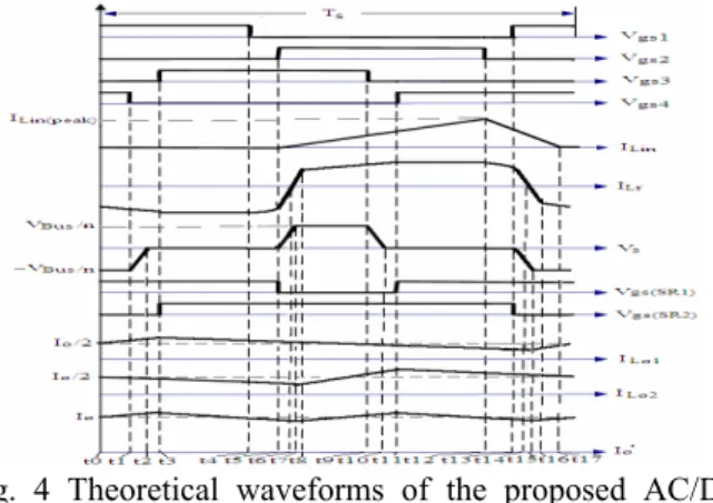
Based on the symbols and signal polarities introduced in Fig. 3, the theoretical waveforms of the proposed converter are shown in Fig. 4. Referring to the equivalent circuits in Fig. 5, the detailed operating principles of the proposed converter are explained as follows:
Mode 1(t0~t1): The power switches Q1 and Q4 remain
turned on, the current that flows through the resonant inductor Lr and the primary winding of power transformer
is equal to -ILo1/n, the first output inductance current ILo1
referred to on the primary side. Corresponding synchronous switch SR1 conduction ensures that the output rectification losses are low. The current ILo1 of the
first output inductor Lo1 flows through SR1 and the
transformer secondary winding, closing the loop through the output capacitor Co. The current ILo1 ramps up linearly
while ILo2 ramps down linearly. The transformer
secondary winding carries only approximately half of the output current and ripple currents cancelled on common output capacitor Co.
Mode 2(t1~t2): Q4 is turned off at t1, the freewheeling
current ILr starts to charge Cp4 and discharge Cp3. Thus,
the drain to source voltage Vds4 across the power switch
Q4 increases and the drain to source voltage Vds3 across
the power switch Q3 decreases.
Mode 3(t2~t3): Until t2 the decreased voltage Vds3 falls
to zero, the voltage on both the primary and secondary windings become zero. The freewheeling current ILr keep
flowing through the anti-parallel diode D3 of the power switch Q3 to ensure the zero voltage turn-on for Q3.
Mode 4(t3~t4): As long as the power switch Q3 is turned
on at t3 before the inductor current ILr changes its
direction, zero-voltage switching can be assured. Corresponding synchronous switch SR2 conduction ensures that the output rectification losses are low. The current Io’ freewheels through the synchronous switches
SR1 and SR2. The voltage across Lo1 also becomes
negative, and equals the output voltage amplitude. Therefore the current ILo1 ramps down like the current
ILo2.
Mode 5(t4~t5): When Q1 is turned off at t4, the resonant
inductor Lr starts to resonate with the parasitic
capacitances Cp1 and Cp2 of the power switches Q1 and
Q2. The resonant current ILr starts to charge Cp1 and
discharge Cp2.
Mode 6(t5~t6): Until t5 the decreased voltage Vds2 falls
to zero and the DC bus voltage forces the inductor current ILr to start commutation.
Mode 7(t6~t7): As long as power switch Q2 is turned on
before the inductor currentILr changes its direction at t6
and zero-voltage switching can be assured. Thus, the ZVS conditions for the power switch Q2 can be determined as follows: ) C C ( L 2 V ) 5 t ( I L T r p1 p2 Bus Lr r max , d ≤ +π + , (1) 2 ) 3 t ( Lr Bus 2 p 1 p r (C C ) IV L ⎟⎟ ⎠ ⎞ ⎜ ⎜ ⎝ ⎛ × + ≥ , (2)
On the secondary side, synchronous switch SR1 is turned off and the freewheeling current flows through the corresponding body diode DS1. During this interval, the DC bus voltage remains to force the inductor current ILr
increasing. At t7, ILr is equal to ILo2/n, the second output
inductance current referred to on the primary side. The body diode DS1 of synchronous switch SR1 is then released.
Mode 8(t7~t8): The inductor current ILr starts to charge
the stray transformer winding capacitor. The resonance caused by inductor Lr and the stray capacitor could be
clamped while the ring-free diode Da is conducted. The current ILo2 of the secondary output inductor Lo2 flows
through SR2 and the transformer secondary winding, closing the loop through the output capacitor Co. The
current ILo2 ramps up linearly while ILo1 ramps down
linearly. When Q2 is zero-voltage turned on, the voltage across the input inductor Lin is equal to the rectified input
voltage |Vin| such that the input inductor current ILin
increases linearly.
Modes 9~12(t8~t12): At t8, Da is released due to the
inductance current ILr stays at ILo2/n. During modes 9~12,
the zero-voltage-switching for the power switch Q4 can be also achieved as similar as modes 1~4. In this interval, the input inductor current |ILin| remains to increase
linearly.
Modes 13~16(t12~t16): When the drain to source voltage
Vds2 across the power switch Q2 increases and then the
voltage across the input inductor Lin decreases to zero, the
input inductor current, ILin reaches its peak. Assuming AC
sinusoidal source voltage Vin(t)=Vmsin(2πfit) and the
dead-time interval is enough short to be negligible, the peak input inductor current, ILin(peak) of each switching
cycle can be expressed as
in s i m ) peak ( in L |V 2sin(f L2 f t)| I = π , (3)
where fs is the switching frequency and fi is the line
frequency. When Q1 is zero-voltage turned on and SR2 is turned off, the resonance caused by inductor Lr and the
transformer stray capacitor could be clamped while the ring-free diode Db is conducted. The voltage across the input inductor Lin is equal to (|Vin|-Vbus) such that the
rectified input current |ILin| decreases linearly and finally
reaches zero at t17. The circuit will then proceed back to mode 1 after completing one operating cycle Ts.
Fig. 4 Theoretical waveforms of the proposed AC/DC converter
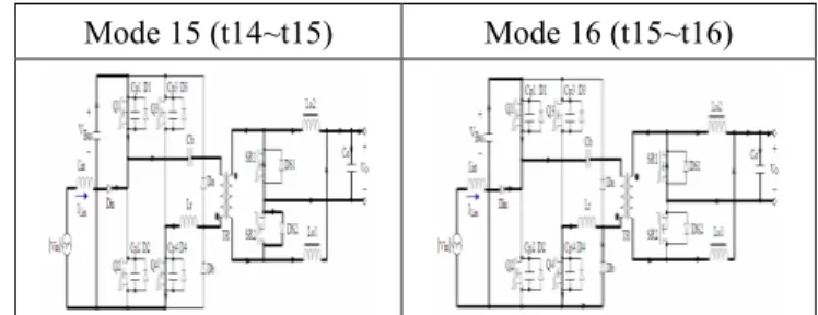
Mode 1 (t0~t1) Mode 2 (t1~t2) Mode 3 (t2~t3) Mode 4 (t3~t4) Mode 5 (t4~t5) Mode 6 (t5~t6) Mode 7(t6~t7) Mode 8 (t7~t8) Mode 9 (t8~t9) Mode 10 (t9~t10) Mode 11 (t10~t11) Mode 12 (t11~t12) Mode 13 (t12~t13) Mode 14 (t13~t14) Mode 15 (t14~t15) Mode 16 (t15~t16)
Fig. 5 Equivalent circuits for different switching modes
III. Steady-State Analysis
In following analysis, the dead-time interval is assumed negligible. The output inductors are operated in the continuous conduction mode (CCM) and are large enough so that current ripples on them are negligible. When the two diagonally placed primary switches (either Q1 and Q4 or Q2 and Q3) keep conducting during active interval δTs, energy is transferred from the input voltage
source through the corresponding conducting synchronous switch (SR1 or SR2) to the load. The source current can be shaped automatically to follow the source voltage by designing the input inductor to operate at DCM. With phase-shifted control, the gating signal for power switch, Q2 always has a 50% duty cycle. The average input inductor current, ILin(on) during on-time of
Q2 and the average input inductor current, ILin(off) during
off-time of Q2 can be expressed as follows:
in s in ) on (, in L 8f L V I = , (4) ) V V ( L f 8 V I in Bus in s 2 in ) off (, in L = − , (5)
The expressions for the average input inductor current, ILin(av) of each switching cycle and the average
input power, Pin(av) are as follows:
) t f 2 sin( M M L f 8 V I i PFC PFC in s in ) av (, in L = − π , (6) θ × ∫ π = π(V I )d 2 1 Pin(av) 02 in Lin(av) θ θ × ∫ π = π(V I )d d 2 1 ) av ( Lin 2 0 in θ ∫ − θθ π = π )d sin M sin M ( L f 4 V /2 0 PFC 2 PFC in s 2 m , (7) m Bus PFC V V M = , (8)
where MPFC is the voltage transfer ratio of the PFC cell at
peak input voltage, Vm. The output power, Po can be
represented by Equation (9). In steady-state, the output power Po should be equal to the average input power
Pin(av). Thus, the voltage transfer ratio MAC/DC of the
proposed single-stage AC/DC converter can be expressed as Equation (11). L 2 o o R V P = , (9)
n V V M Bus o DC / DC = = δ, (10) m o DC / AC VV M = θ ∫ − θθ π = π )d sin M sin M ( L f 4 R /2 0 PFC 2 PFC in s L ,(11)
where RL is the load resistance of the AC/DC converter. IV. Design Considerations
A. Control Design
A modified phase-shifted control method is used to regulate output voltage of the single-stage AC/DC converter. Figure 6 shows a schematic diagram of the proposed control circuit. The phase-shifted PWM control signals can be produced using commercialized control ICs, such as UC3879. The voltage regulation for the DC/DC cell can be achieved by varying the phase-shift between the two legs of the bridge circuit. However, the gating signal for power switch, Q2 always has a 50% duty cycle. The DC bus voltage in the proposed single-stage AC/DC converter cannot be regulated by conventional phase-shifted control method. Based on Equation (7), a variable frequency control circuit then is added to vary the input power of PFC cell by adjusting the switching frequency. The power balance for the single-stage AC/DC converter can be achieved by regulating the DC bus voltage as shown in Fig. 6. A DC bus protection circuit was also implemented. When the voltage feeding back from the DC bus reaches the upper voltage, VU, the power
switch Q2 is turned off to protect the DC bus until the feedback voltage is less than the lower voltage, VL.
Synchronous switches SR1 and SR2 can be controlled by using self-driven and external-driven methods. The merits of the self-driven configuration are ease of implementation and fewer components. However, the critical drawback of large variation in Rds(on) depending on
operating conditions does exist [9, 10]. To fully benefit from synchronous rectification, the external-driven approach was adopted and the conduction criteria for the synchronous switches SR1 and SR2 involves replacing the corresponding anti-parallel diodes DS1 and DS2 in the high current path. The control logic for synchronous switches SR1 and SR2 can be determined from 16 combinations of switching states as shown in Table 2, where “1” represents turned-on, “0” represents turned-off and “x” means neutral. When the synchronous switch state is marked neutral, this state will not occur in a practical circuit. However, the switch can still be logically turned off without affecting the circuit operations. If we replace "x" in the Table 2 with "0", the look-up table dimensions can be greatly reduced. From Table 2, the gating signals for SR1 and SR2 can be derived and simplified as follows: 4 Q 2 Q 1 SR = ⋅ , (12) 3 Q 1 Q 2 SR = ⋅ , (13)
In practical implementation, SR1 (SR2) must be turned off before Vs goes from zero to the positive
(negative) level in order to avoid a current spike through the transformer winding and both SRs, causing unnecessary power loss. When Vs goes from positive
(negative) level to zero, SR1 (SR2) will remain off until Q4 (Q3) is turned on to avoid the shoot-through. The simulation waveforms are shown in Fig. 7(a) to verify the feasibility of the proposed gating logic for the synchronous switches.
B. Inductor Design
Based on the design criteria proposed in [12], the input inductor Lin must satisfy the condition as follow:
s ) DC / DC ( in 3 PFC PFC 2 PFC in 2f R M ) 92 . 0 M ( ) 1 M ( 48 . 0 L − − ≤ , (14)
where Rin(DC/DC) is the equivalent input resistance of the
DC/DC cell. From Equation (9), we can obtain the equivalent input resistance Rin(DC/DC) for the DC/DC cell:
2 DC / DC L ) DC / DC ( ) DC / DC ( in M R R =η , (15)
where η(DC/DC) is the efficiency of the DC/DC cell.
Combining (14) and (15), we can determine the input inductor Lin. 2 DC / DC s L ) DC / DC ( 3 PFC PFC 2 PFC in M f 2 R M ) 92 . 0 M ( ) 1 M ( 48 . 0 L η − − ≤ , (16)
As previously mentioned, when two primary switches on the same side of the bus trail (either Q1 and Q3 or Q2 and Q4) keep conducting during the passive interval (1-δ)Ts, the transformer windings are shortened
due to conduction in the synchronous switches (SR1 and SR2). The proposed current doubler synchronous rectifier shown in Fig. 7(b) can be equivalent to Fig. 7(c) during these passive intervals. Thus, the relationship between output current ripple ∆Io(pk-pk) and equivalent output
inductor Leq can be expressed by:
eq (min) s o ) pk pk ( o f(1 )LV I ≤ −δ ∆ − , (17) 2 o 1 o eq L //L L = , (18)
where fs(min) is the minimum switching frequency of the
primary switches. For the given output current ripple specification, the output inductors Lo1 and Lo2 can be
realized with the same inductance Lo and determined by:
) pk pk ( o (min) s o o f 2(1 I )V L − ∆ δ − ≥ , (19)
Fig. 6 The schematic diagram of the proposed control circuit
(a)
(b) (c)
Fig. 7(a) The simulation waveforms for verifying the gating logic of the synchronous switches(b) Current doubler synchronous rectification (c) Equivalent circuit in passive intervals
V. Simulation and Experimental Verification
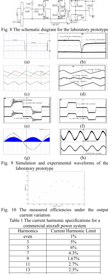
To verify the feasibility of the proposed single-stage AC/DC converter, a laboratory prototype as shown in Fig. 8 was built to convert a 115Vrms/400Hz source into
5VDC/100A output for the PAS antenna. The design
procedure for the prototype is summarized as follows: Select a nominal duty ratio δ=0.25 and an average DC bus voltage VBus=400V. Based on Equation (10), the
parameter MDC/DC and transformer turn ratio, n can be
determined as 0.0125 and 20. From the input voltage specification, the parameter MPFC can be calculated as
2.46. We assumed η(DC/DC)=90%, the input inductance Lin
can be selected as 130µH according to Equation (16). The maximum input inductor current, ILin(max) is determined as
approximately 12.5A. Select power MOSFETs IRF460 as the common switch Q2, IRF840 as the other primary switches Q1, Q3 and Q4, then find the parasitic capacitances from the datasheet: Cp2=870pF and
Cp1=Cp3=Cp4=310pF. From Equation (2), a resonant
inductance Lr is selected as 47µH. Typically, the ripple
currents on the output inductors are requested at about 25% of the full load current. Therefore, the output inductance can be determined as Lo1=Lo2=6µH. The
circuit parameters of this design example are listed Table 3. Fig. 9 shows the simulation and experimental results to verify the feasibility. Figures 9(a) and (b) show the simulation and experimental waveforms illustrating the ZVS feature. Figures 9(c) and (d) show the simulation and experimental waveforms of the output-side currents ILo1, ILo2 and Io’. Ripple cancellation between the two
output inductor currents was observed. Figures 9(e) and (f) illustrate the suppression of parasitic ringing by the addition of ring-free diodes. It is clear that the parasitic ringing could be reduced. The snubber circuits, which cause additional power dissipation, are not required. Because of parasitic ringing suppression, the EMI feature of the proposed converter could be improved. Figure 9(g) shows the simulation waveforms of the AC source voltage Vin and inductor current ILin. Figure 9(h) depicts the
filtered 400 Hz source voltage Vin and current Iin
waveforms of the laboratory prototype. By adding a small filter capacitor, the proposed converter shows a high power factor and low current harmonics features. Figure 10 shows the measured efficiencies of the proposed AC/DC converter under the output current variation. It is clear that the conversion efficiency can be greatly
improved.
Fig. 8 The schematic diagram for the laboratory prototype
(a) (b) (c) (d) (e) (f) (g) (h)
Fig. 9 Simulation and experimental waveforms of the laboratory prototype
Fig. 10 The measured efficiencies under the output current variation
Table 1 The current harmonic specifications for a commercial aircraft power system Harmonics Current Harmonic Limit
even 1% 3 5% 5 6% 7 4.3% 9 1.67% 11 2.7% 13 2.3% 15 1% 17 1.8% 19 1.6% 21 0.7% 23 1.3% 25 1.2% <2.5µF per phase per kVA capacitance allowed
Table 2 Switching states of the synchronous switches (SR1 SR2) Q3 Q4 Q1 Q2 0 0 0 1 1 1 1 0 0 0 (x x) (1 1) (x x) (1 1) 0 1 (0 1) (1 1) (x x) (0 1) 1 1 (x x) (x x) (x x) (x x) 1 0 (1 0) (1 0) (x x) (1 1) Table 3 The circuit parameters of a design example
Parameter Symbol Value Source voltage Vin 115Vrms
Line frequency fi 400Hz
Output voltage Vo 5Vdc
Output current Io 100A
Input inductor Lin 130µH
Output inductor Lo1, Lo2 6µH
External resonant
inductor Le 17µH
Transformer turn ratio n 60:3 Transformer leakage
inductance Ll 30µH
DC bus capacitor Cdc 470µF
Output capacitor Co 8800µF VI. Conclusion
In this paper, a high efficiency single-stage AC/DC converter for commercial aircraft power system applications was introduced. The input current harmonics and conversion efficiency could be greatly improved by employing the proposed single-stage topology. The proposed PAS power system has ring-free and low EMI features. Detailed operating principles and design criteria for the proposed converter were described. The IsSpice simulation and performance measurement of a laboratory prototype were performed to verify the feasibility of the proposed method. The results were satisfactory.
Acknowledgment
The authors would like to acknowledge the financial support of the National Science Council of Taiwan, R. O. C. through grant number NSC 93-2213-E033-009.
References
[1] R. Bachik, A. Brockschmidt, C. Epperson, Y. King, “Practical Aspects of Line-Line and Line-Gground Single Phase PFC,” IEEE APEC’99, Vol. 1, pp. 342-348.
[2] R. Redl, N. O. Sokal, and L. Balogh, “A Novel Soft Switching Full Bridge DC/DC Converter: Analysis, Design Considerations, and Experimental Result at 1.5kW, 100kHz,” IEEE PESC’90, pp. 162-172. [3] J. A. Sabate, V. Vlatkovic, R. B. Ridley, F. C. Lee,
and B. H. Cho, “Design Considerations for High-Voltage High-Power Full-Bridge Zero-Voltage-Switched PWM Converter,” IEEE APEC’90, pp. 275-284.
[4] G. C. Hsieh, J. C. Li, and M. H. Liaw, “A Study on
Full-Bridge Zero-Voltage-Switched PWM Converter: Design and Experimentation,” IEEE IECON’93, pp. 1281-1285.
[5] J. W. Baek, J. G. Cho, D. W. Yoo, G. H. Rim, and H. G. Kim, “An Improved Zero Voltage and Zero Current Switching Full Bridge PWM Converter with Secondary Active Clamp,” IEEE PESC’98, pp. 948-954.
[6] S. Valtchev, and B. V. Borges, “Improved Full Bridge Zero Voltage Switched Phase Shift DC/DC Converter Using a Secondary Clamped Inductor,” IEEE IECON’95, vol. 1, pp.258-264.
[7] W. Chen, F. C. Lee, M. M. Jovanovic, and J. A. Sabate, “A Comparative Study of a Class of Full Bridge Zero-Voltage-Switched PWM Converters,” IEEE APEC’95, vol.2, pp. 893-899.
[8] N. H. Kutkut, “A Full Bridge Soft Switched Telecom Power Supply with a Current-Doubler Rectifier”, IEEE INTELEC’97, pp. 344-351.
[9] G. Stojcic, and C. Nguyen, “MOSFET Synchronous Rectifiers for Isolated, Board-Mounted DC-DC Converters”, IEEE INTELEC’00, pp. 258-266.
[10] Li Xiao, and R. Oruganti, “Soft Switched PWM DC/DC Converter with Synchronous Rectifiers”, IEEE INTELEC’96, pp. 476-484.
[11] J. A. Cobos, J. Sebastian, J. Uceda, E. de la Cruz, and J. M. Gras, “Study of the Applicability of Self-Driven Synchronous Rectification to Resonant Topologies”, IEEE PESC’92, pp. 934-940.
[12] D. Simonetti, J. Sebastian, A. Cobos and J. Uceda, “Analysis of the Conduction Boundary of a Boost PFP fed by Universal Input”, IEEE PESC’96, pp. 1204-1208.