P1-7 / W.-S.Choi
IMID 2009 DIGEST •
Abstract
With injection-type source delivery system of atomic layer deposition (ALD), bottom-contact and bottom-gate thin-film transistors (TFTs) were fabricated with a poly-4-vinyphenol polymeric dielectric for the first time. The properties of the ZnO TFT were greatly influenced by the device structure and the process conditions. The zinc oxide TFTs
exhibited a channel mobility of 0.43 cm2/Vs, a
threshold voltage of 0.85 V, a subthreshold slope of
3.30 V/dec, and an on-to-off current ratio of above 106
with solid saturation.
1. Introduction
Research efforts on ZnO thin film have driven by its characteristic and potential applications. ZnO has a wide band and direct band gap II-VI semiconductor. The various applications include transparent conductor, solar cell window, ultraviolet light emitter, gas sensors, photovoltaic devices, and surface acoustic wave devices. Its wide applications owes to its its properties such as wide direct band gap of 3.4 eV at room temperature, large exciting binding energy of 60 meV at RT, high optical transparency in the visible region, good electrical conductivity and outstanding piezoelectricity. ZnO thin films have been prepared by various technologies such as sputtering [1], metal oxide chemical vapor deposition [2], pulse laser deposition [3], sol-gel process [4], spray pyrolysis [5], and atomic layer deposition (ALD) [6].
Zinc-oxide (ZnO) thin-film transistors were prepared by using different techniques. Previous results with inorganic dielectric materials were reported, and most of them used a sputtering technique to prepare the active channel material. A top-ZnO TFT with a polymeric dielectric by using r.f.
sputtering at 100oC was fabricated [7]. Other used the
atomic layer deposition (ALD) technique for ZnO preparation. Also inorganic dielectrics, such as aluminium oxide, mostly used for the devices. However, there have been no reports on an oxide semiconductor with a polymeric gate dielectric fabricated by using ALD.
In this work, a gate and bottom-contact ZnO TFT with a polymeric dielectric material was fabricated. The ZnO thin-film was deposited by using the ALD technique and was patterned. The polymer dielectric was spin-coated and dry-etched. The thermally-annealed ZnO TFT was characterized.
2. Experimental
The bottom-gate and bottom-contact ZnO TFT was prepared as follows. Indium tin oxide (ITO)
as a gate metal was patterned on 100X100 mm2 glass
by using photolithography. Poly-4-vinylphenol (PVP) was spin coated with a crosslinking agent on an ITO-patterned glass substrate and cured in a vacuum oven to have a 450 nm thickness. The dielectric pattern was dry-etched by for the contact open. Gold as a source and a drain was deposited on the substrate by using thermal evaporator and was patterned by using a lift-off process. The ZnO thin film used as a channel material was deposited on the cleaned substrate by using ALD with an injection type source delivery
system at a temperature of 150oC. As a source of Zn,
diethylzinc was used. An oxygen plasma was used as an oxygen source for ZnO fabrication. The reactor pressure was maintained 0.7 Torr with argon gas purging at 100 sccm. During the reaction, diethylzinc and the oxygen plasma were sequentially injected into the reactor chamber to form a ZnO monolayer on the substrate. The active layer was patterned by using photolithography. The TFT channel was 10-μm width and 10-μm length. The thermal treatment of ZnO TFT
ZnO Thin Film Transistor Prepared from ALD
with an Organic Gate Dielectric
Woon-Seop Choi*
School of Display Engineering, Hoseo University, Asan-City, Chungnam, 336-795, Korea Tel.:82-41-540-5924, E-mail: [email protected]
P1-7 / W.-S.Choi
• IMID 2009 DIGEST
was carried out in a hot plate chamber under an
oxygen atmosphere at 200oC for 1 hour. All current
voltage (I-V) characterizations of the ZnO TFT were carried out with a semiconductor parameter analyzer (Keithley 4200) in the dark at room temperature.
3. Results and discussion
In order to make oxide TFT with bottom-contact and bottom-gate, ITO and gold (Au) were used as electrode materials, and patterned by lithography and lift-off process, respectively, to obtain better design rule instead of the shadow mask. The ZnO thin film prepared by ALD was patterned by photolithography to obtain 10 μm of channel length.
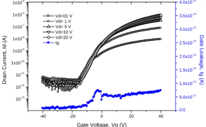
The transfer characteristics of ALD prepared ZnO TFT with different statues such as as-deposition, thermal treatment, and stored with time are shown. Fig. 1 plots a set of log(Id) vs. Vg transfer curves with different ranges of Vd from 100mV to 20V. The 10 and 20V curves are typical of such transfer characteristics, where Vd is sufficiently large so that the device operations are in saturation state with the ranges of applied gate voltages. With different drain voltages, 100 mV to 20 V, the transition characteristics of the transfer curves show typical transfer regions from linear operation regions to saturation regions. The corresponding output characteristics are shown in Fig 2. In particular, the 100-mV curve and the 1-V curve are separated by almost one decade. The separation between the 1-V and the 5-V curves is almost a decade which is smaller than for 100-mV and 1-V curves. However, from the 5-V curve, the separation is much smaller, and the 5-, 10-, 20-V curves are almost overlaid upon one another. For this device, therefore, the transition from linear operation to saturation occurs for Vd between 1 V and 5 V.
The threshold voltage (Vth) and the saturation mobility were obtained by fitting the straight line of the square root of Id versus Vg from Fig. 1. The
mobility is about 0.43 cm2/Vs for 10 μm X 10μm
device. From this transfer characteristic, the turn on gate voltage (Vth) shows approximately 0.85 V. The subthreshold slope is 3.30 V/dec. The ZnO TFT operates in depletion mode.
In Fig 2, a set of drain current-voltage (Id-Vd) curves for discrete gate voltages (Vg) between 0 to 40 V for a fabricated ZnO TFT with a polymeric dielectric
exhibit linear region to saturation region characteristics like well operated general TFT systems.
-40 -20 0 20 40 10-13 10-12 10-11 1x10⁻¹⁰ 1x10⁻⁹ 1x10⁻⁸ 1x10⁻⁷ 1x10⁻⁶ 1x10⁻⁵ Vd=01 V Vd= 1 V Vd= 5 V Vd=10 V Vd=20 V Ig Gate Voltage, Vg (V) D ra in Curre nt , Id (A) 0.0 5.0x10⁻¹¹ 1.0x10⁻¹⁰ 1.5x10⁻¹⁰ 2.0x10⁻¹⁰ 2.5x10⁻¹⁰ 3.0x10⁻¹⁰ 3.5x10⁻¹⁰ 4.0x10⁻¹⁰ G a te Le aka g e , Ig (A)
Fig. 1. Transfer characteristics of bottom-gate, bottom-contact, ALD-grown ZnO TFT with different drain voltages (Vd), (W/L=10 μm/10 μm).
0 5 10 15 20 25 30 -5.0x10⁻⁸ 0.0 5.0x10⁻⁸ 1.0x10⁻⁷ 1.5x10⁻⁷ 2.0x10⁻⁷ 2.5x10⁻⁷ 3.0x10⁻⁷ 3.5x10⁻⁷ 4.0x10⁻⁷ 4.5x10⁻⁷ 5.0x10⁻⁷ Drain C u rr ent , Id (A) Drain Voltage, Vd (V) Vg= 0 V Vg= 5 V Vg=10 V Vg=15 V Vg=20 V Vg=25 V Vg=30 V Vg=35 V Vg=40 V
Fig. 2. Output characteristics of bottom-gate, bottom-contact, ALD-grown ZnO TFT with different gate voltages (Vg), (W/L=10 μm/10 μm).
4. Summary
With an injection type source delivery system, a very short injection time for precursor delivery was chosen for the preparation of a ZnO film by using ALD. For the first time, a bottom-contact TFT with a ZnO semiconductor with a poly-4-vinyphenol polymeric dielectric was successfully fabricated by using ALD. The ZnO TFT was operated in the depletion mode. The TFT properties were greatly influenced by the device structure and the process conditions. Thermal annealing of the ZnO TFT
P1-7 / W.-S.Choi
IMID 2009 DIGEST •
improved its electric characteristics. The electrical properties of the oxide TFT were a channel mobility
of 0.43 cm2/Vs, a threshold voltage of 0.85 V, a
subthreshold slope of 3.30 V/dec, and an on-to-off
current ratio of above 106 with a low off-current of
around 10-12 A.
Acknowledgement
The author thanks Professor J. Jang and his students at Kyunghee University for the gate dielectric patterning and for valuable conversations.
5. References
[1] Y. Zho, P.J. Kelly, A. Postill, O.A. Zeid, A.A.
Alnajjar, Hin Soild Films, 447-448, p.33 (2004)
[2] O. Pagni, N.N. Somhlalo, C. Weichesel, A.W.
Leitch, Physica B, 376-377, p.305 (2006)
[3] V. Cracium, J. Elders, J.G. Gardeniers, I.W.
Boyd, Appl. Phys. Lett., 65, p.2963 (1994)
[4] W Tang, D.C. Cameron, Thin Solid Films, 238,
p.83 (1994)
[5] T.Y. Ma, S,C, Lee, J. Mater. Sci. Mater. Electron.
11, p.305 (2000)
[6] S.H. Park, C.S.Hwang, H.S. Kwack, J.H. Lee,
H.Y. Chu, Electrochem. And Solid-state Lett., 9, p.G229 (2006)
[7] K. Lee, J. H. Kim, and S. Im, Appl. Phys. Lett. 88,