ICCAS2005 June 2-5, KINTEX, Gyeonggi-Do, Korea
Robust Control of DC-DC Converter by Approximate 2DOF Digital Controller
Realizing First-Order Model
Kohji HIGUCH∗, Eiji TAKEGAMI∗∗, Kazushi NAKANO∗, Satoshi TOMIOKA∗∗ and Kazushi WATANABE∗∗
∗The University of Electro-Communications, 1-5-1 Chofu-ga-oka, Chofu, Tokyo 182-8585, Japan (Tel: +81-424-43-5182; Fax: +81-424-43-5183; Email:[email protected])
∗∗DENSEI-LAMBDA K.K., 2701 Togawa, Settaya, Nagaoka 940-1195, Japan (Tel: +81-258-22-3663; Fax: +81-258-22-3704; Email:[email protected])
Abstract: Robust DC-DC converter which can cover extensive load changes and also input voltage changes with one controller is needed. In this paper, we propose a method for determining the parameters of 2DOF digital controller which makes the control bandwidth wider, and at the same time makes a variation of the output voltage very small at sudden changes of resistive load and the input voltage. The 2DOF digital controller whose parameters are determined by the proposed method is actually implemented on a DSP and is connected to a DC-DC converter. Experimental studies demonstrate that this type of digital controller can satisfy given specifications.
Keywords: DC-DC converter, Digital integral-type control system, First-order model, Approximate 2DOF system, Robust control
1. Introduction
In many applications of DC-DC converters, loads cannot be specified in advance, i.e., their amplitudes are suddenly changed from the zero to the maximum rating. Gener-ally, design conditions are changed for each load and then each controller has to be re-designed. Then, a so-called ro-bust DC-DC converter which can cover such extensive load changes and also input voltage changes with one controller is needed. Analog control IC is used usually for the controller of DC-DC converters. Simple integral control etc. are per-formed with the analog control IC. Moreover, the applica-tion of the digital controller to DC-DC converters designed by the PID or root locus method etc. has been considered recently[1], [2]. However it is difficult to retain sufficient ro-bustness of DC-DC converters by these techniques.
The authors proposed the method of designing an approxi-mate 2-degree-of-freedom (2DOF) robust controller of DC-AC converters[3], [4]. For applying this approximate 2DOF controller to DC-DC converters, it is necessary to improve the degree of approximation for better robustness. The au-thors also proposed the method of designing an approxi-mate 2-degree-of-freedom (2DOF) robust controller of DC-DC converters using a second-order model[5]. In this pa-per, we propose a new method for designing good approxi-mate 2DOF digital controller using a first-order model which makes the control bandwidth wider, and at the same time makes a variation of the output voltage very small at sud-den changes of resistive load. We also show the controller parameter design procedure which performs good approxi-mation. This type of good approximate 2DOF controller is constituted as follows : First, a model matching system with a specified rising time in startup transient response is constituted by using the voltage and the current feedbacks. The current sensor is generally expensive and noisy. In or-der to avoid use of the current sensor, the current feedback is changed by using a dynamic compensator into the output This paper is supported by CAMPUS CREATE Co.,Ltd..
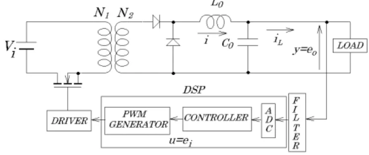
Fig. 1. DC-DC converter
feedback and control input feedback equivalently. Secondly, a first order approximate model of this model matching sys-tem is derived. And inverse syssys-tem of this first order ap-proximate model and a filter for realizing the inverse system are combined with the model matching system. Finally, an equivalent conversion of the portion of the controller is car-ried out, and a realizable approximate 2DOF controller is obtained. This digital controller is actually realized by using a DSP. Some simulations and experiments show that the pro-posed high-order approximate 2DOF digital controller can satisfy given specifications.
2. DC-DC converter
The DC-DC converter as shown in Fig.1 has been manu-factured. In order to realize the approximate 2DOF dig-ital controller which satisfies given specifications, we use T IT M S320LF 2401 as DSP. This DSP has a built-in AD converter and a PWM switching signal generating part. The triangular wave carrier is adopted as a PWM switching signal generating part. The switching frequency is set at 300[KHz] and the peak-to-peak amplitude Cmis 66[V]. The LC circuit is a filter for removing carrier and switching noises. L0 is 1.4[µH], and C0 is 308[µF]. If the frequency of control in-put u is smaller enough than that of the carrier, the state equation of the DC-DC converter at resistive load in Fig.1
ex-Fig. 2. Controlled object with input dead time Ld(≤ T ) cept DSP can be expressed from the state equalizing method (Fukuda and Nakaoka, 1993) as follows:
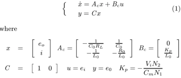
n ˙x = A cx + Bcu y = C x (1) where x = · eo i ¸ Ac= · − 1 C0RL 1 C0 −L10 − R0 L0 ¸ Bc= · 0 Kp L0 ¸ C = £ 1 0 ¤ u = ei y = e0 Kp=− ViN2 CmN1 When realizing a digital controller by a DSP, a delay time exists between the start point of sampling operation and the output point of control input due to the input computing time and AD/DA conversion times. This delay time is con-sidered to be equivalent to the input dead time which exists in the controlled object as shown in Fig.2.
Then the state equation of the system of Fig.2 is expressed as follows: n x dw(k + 1) = Adwxdw(k) + Bdwv(k) y(k) = Cdwxdw(k) (2) where xdw(k) = · xd(k) ξ2(k) ¸ xd(k) = · x(k) ξ1(k) ¸ Adw = · Ad Bd 0 0 ¸ Bdw= · 0 1 ¸ Ad = · eAcT eAc(T−Ld)RLd 0 e AcτB cdτ 0 0 ¸ Bd = · RT−Ld 0 e AcτB cdτ 1 ¸ Cdw = £ Cd 0 ¤ Cd = £ C 0 ¤ ξ1(k ) = u(k ) In practical use of DC-DC converter, the characteristics of a startup transient response and a dynamic load response are important. The DC-DC converter with the following specifi-cations (1)-(6) is designed and manufactured by constituting digital controller to DC-DC switching part.
1. Input voltage Vi is 48[V] and output voltage eo is 3.3[V].
2. Startup transient reponses are almost the same at re-sistive load and parallel load of resistance and capacity, where 0.165≤RL<∞[Ω], 0≤CL≤200[µF].
3. The rising time in startup transient reponse is smaller than 100[µs].
4. Against all the loads of spec.2, an over-shoot is not allowable in startup transient response.
Fig. 3. Equivalent disturbances due to load variations (pa-rameter variations) and model matching system with state feedback
5. The dynamic load response is smaller than 50[mV] against 10[A] change of load current.
6. The specs. (2),(3),(4) and (5) are satisfied also to change of input voltage of±20%.
The load changes for the controlled object and the input volt-age change are considered as parameter changes in eq.(2). Such parameter changes can be transformed to equivalent disturbances qv and qy as shown in Fig.3 even in discrete-time systems. Moreover, if the saturation in the input arises or the input frequency is not so small as the carrier fre-quency, the controlled object will be regarded as a class of nonlinear systems. Such characteristics changes can be also transformed to equivalent disturbances as shown in Fig.3. Therefore, what is necessary is just to constitute the con-trol systems whose pulse transfer functions from equivalent disturbances qv and qy to the output y become as small as possible in their amplitudes, in order to robustize or suppress the influence of these parameter changes, i.e., load changes, and input voltage change. In the next section, an easily designing method which makes it possible to suppress the influence of such disturbances with the target characteristics held will be presented.
3. Design of good approximate 2DOF digital integral-type control system
First, the transfer function between the reference input r and the output y is specified as follows:
Wry =
(1 + H1)(1 + H2)(1 + H3)(z− n1)(z− n2)(z + H4) (1− n1)(1− n2)(z + H1)(z + H2)(z + H3)(z + H4)
(3) where, n1 and n2 are the zeros for discrete-time control ob-ject (2). It shall be specified that the relation of H1 and H2, H3 becomes |H1|À|H2| and |H3|. Then Wry(z) can be approximated in the following manner:
Wry(z)≈ Wm(z) = 1 + H1 z + H1
(4) This target characteristic Wry(z)≈ Wm(z) is specified to satisfy the specs.(3) and (4).
Fig. 4. Model matching system using only voltage (output) feedback
Applying a state feedback
v = −F x∗+ GH4r (5) x∗ = [y x2 ξ1 ξ2]T
and feedforward
ξ1(k + 1) = Gr (6)
to the discrete-time controlled object as shown in Fig.3, we decide F = [F (1, 1) F (1, 2) F (1, 3) F (1, 4)] and G so that Wry(z) becomes eq.(3). Th current feedback is used in Fig.3. This is transformed to voltage and control input feedbacks, without changing the pulse transfer function between r−y by an equivalent conversion. The following relation is obtained from Fig.3: −F (1, 2)x2(k) = − F (1, 2) Ad(1, 2) (x1(k + 1) −Ad(1, 1)x1(k) − Ad(1, 3)ξ1− Bd(1, 1)η) (7) If the current feedback is transformed equivalently using the right-hand side of this equation, the control system with only voltage feedback as shown in Fig.4 will be obtained. The transfer function WQy(z) between this equivalent distur-bance Q = [qv qy]T and y of the system in Fig.4 is desfined as WQy(z) = £ Wqvy(z) Wqyy(z) ¤ (8) The system added the inverse system and filter to the sys-tem in Fig.4 is constituted as shown in Fig.5. In Fig.5, the transfer function F (z) becomes
F (z) = kz z− 1 + kz
(9) The transfer functions between r−y and Q− y of the system in Fig.5 are given by
y = (1 + H1) (z + H1) z− 1 + kz z− 1 + kzWs(z) Ws(z)r (10) y = z− 1 z− 1 + kz z− 1 + kz z− 1 + kzWs(z) WQy(z)Q (11) where Ws(z) = (1 + H2)(1 + H3)(z− n1)(z− n2) (z + H2)(z + H3)(1− n1)(1− n2) (12)
Fig. 5. System reconstituted with an inverse system and a filter
Fig. 6. Approximate 2DOF digital integral-type control system
Here, if Ws(z)≈ 1, then eqs.(10) and (11) become, respec-tively, y ≈ 1 + H1 z + H1 r (13) y ≈ z− 1 z− 1 + kz WQy(z)Q (14)
From eqs.(13) and (14), it turns out that the characteristics from r to y can be specified with H1, and the characteristics from Q to y can be independently specified with kz. That is, the system in Fig.5 is an approximate 2DOF system, and its sensitivity against disturbances, i.e., load change becomes lower with the increase of kz.
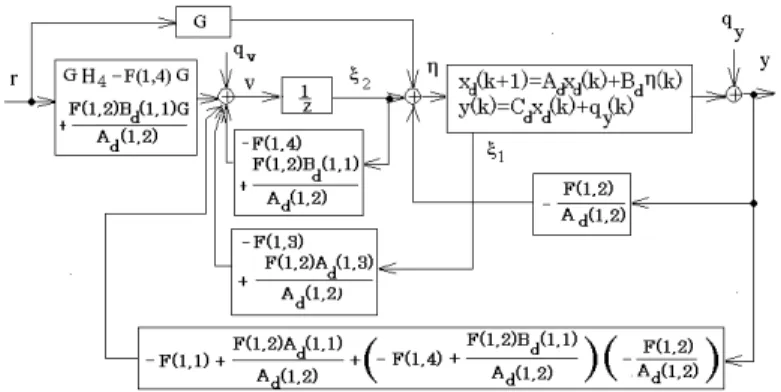
If an equivalent conversion of the controller in Fig.5 is car-ried out, the approximate 2DOF digital integral-type control systems will be obtained as shown in Fig.6. In Fig.6, the parameters of the controller are as follows:
k1 = F (1, 1 + F (1, 2)F F (1, 1) + ((−F (1, 4) − F (1, 2)F F (1, 4))(−F (1, 2)/F F (1, 2))) + (GH4 + GFz)(kz/(1 + H2)) k2 = F (1, 2)/F F (1, 2) + G(kz/(1 + H2)) k3 = F (1, 3) + F (1, 2)(F F (1, 3)) k4=−Fz ki1 = Gkz ki2= (GH4 + GF z)kz kr1 = G kr2= GH4 + GFz (15) where F F (1, 1) = −Ad(1, 1)/Ad(1, 2)
F F (1, 2) = Ad(1, 2)
F F (1, 3) = −Ad(1, 3)/Ad(1, 2) F F (1, 4) = −Bd(1, 1)/Ad(1, 2)
Fz = −F (1, 4) − F (1, 2)F F (1, 4)
Now, for good approximation, i.e., in order to let eqs.(10) and (11) approach further to the right-hand side of eqs.(13) and (14) respectively, what is necessary is just to set up so that Ws(z) may approach to 1 further in the large frequency range. Moreover, it is necessary to make the gain of eq.(14) small for low sensitivity. For the purpose, while the gain of WQy is made small, we have to make kz into large value. However, if kz is enlarged, the roots of following equation in eq.(10) may approach H1, and the degree of approximation may become not so good.
z− 1 + kzWs(z) = 0 (16) The roots of eq.(16) are ones of whole systems except for H1 and H4 . When kz is made to increase from 0, these roots leave 1, −H2, and −H3, and when kz is set as a certain value, they become certain values like p1, p2, and p3. If we determine−H2 and−H3 so that the following equation is satisfied and the absolute value of the real number part of those become small suitably when kz is sufficiently large value, the degree of approximation of eqs.(10) and (11) will become good, and low sensitivity will also become good.
(|Re(p1)|, |Re(p2)|, |p3|) ¿ |H1| (17) If p1, p2, and p3 are specified like eq.(17) and kz is specified to be a suitable value, we can search for starting point H2 and H3 of root loci, reversely. If the roots of eq.(16) are specified to be p1, p2, and p3, the following equation will be obtained from eq.(12) .
(1− n1)(1− n2)(z− 1)(z + H2)(z + H3) +kz(1 + H2)(1 + H3)(z− n1)(z− n2)
= (z− p1)(z− p2)(z− p3) (18) Substituting H2 = x + yi, H3 = x− yi, and the value of kz for eq.(18), and setting the coefficient of of each power of z equally , the equation of three circles about x and y will be obtained. H2 and H3 can be determined from the intersection of these circles. The design procedure of the parameters of the controller is shown as follows:
1. H1is set up so that the specified rising time is satisfied. 2. H4 is set up as
|H4| ≈ 0.5|H1| (19) 3. The roots of eq.(16) are set up as
p1 ≈ −0.5H1+ 0.5H1i p2≈ −0.5H1− 0.5H1i
p3 ≈ −0.5H1 (20)
4. kz of eq.(16) are set up as
kz≈ 0.5 (21)
Fig. 7. Circles of eqs.(27),(28) and (29)
Fig. 8. Simulation results of startup responses at various loads
5. Determin H2 and H3 so that the roots of eq.(16) be-come equal to p1, p2and p3.
6. Determine the parameters of the controller from eq.(15).
7. Check whether all the specifications are satisfied by simulation.
8. When not satisfying the specification, 4. is changed a little and the next 5. are repeated.
9. Furthermore when not satisfying the specification, 3. is changed a little and the next 4. are repeated.
4. Experimental studies
The sampling period T are set as 3.3[µs] and the input dead time Ldis about 0.999T [µs]. We will design a control system so that all the specifications are satisfied. First of all, in order to satisfy the specification on the rising time in startup transient reponse, from design procedures 1. and 2., H1, and
Fig. 9. Simulation result of dynamic load response at resis-tive load
H4 are set as
H1=−0.89 H4=−0.3 (22) In order to increase the degree of the approximation in eqs.(13) and (14) over the large frequency range, what is necessary is just to make the absolute value of the real part of the roots of eq.(16) as small as possible. Substituting
H2= x + yi H3= x− yi (23) into eq.(18), we get
( kzx2+ (2kz− 2n2+ 2n1n2− 2n1+ 2)x + kzy2+ (−1 + n2+ kz− n1n2+ n1))/(1− n2− n1 + n1n2) =−p1− p3− p2 (24) ( (−kzn1+ n1n2− n2+ 1− n1− kzn2)x2 + (2n2+ 2n1− 2kzn2− 2n1n2− 2kzn1− 2)x + (−kzn1+ n1n2− n2+ 1− n1− kzn2)y2 − kzn2− kzn1)/(1− n2− n1+ n1n2) = p1p3+ p1p2+ p2p3 (25) ( (−1 + n2+ kzn1n2− n1n2+ n1)x2 + 2kzn1n2x + (−1 + n2+ kzn1n2 − n1n2+ n1)y2+ kzn1n2)(1− n2− n1 + n1n2) =−p1p2p3 (26) These are circle equations when fixing kz. From procedures 3. and 4., setting as
p1 = 0.35 + 0.5i p2 = 0.35− 0.5i p3 = 0.5 kz = 0.3 n1=−0.97351 n2=−.97731e6
(27) and substituting these into eqs.(24),(25) and (26), we get
2x + 0.0000016x2+ 0.0000016y2+ 0.2 = 0 (28) −1.696x + 1.152x2+ 1.152y2− 0.570 = 0 (29) 0.296x− 0.852x2− 0.852y2+ 0.334 = 0 (30) These circles are drawn in Fig.7. From the intersect point, we get
x =−0.1 y = 0.6 (31)
Fig. 10. Experimental startup response at RL= 0.33[Ω]
Fig. 11. Experimental startup response at RL= 0.165[Ω]
Then, from the procedure 6., the parameters of controller become
k1 = −332.223 k2= 260.57 k3=−0.51638 k4 = −0.51781 ki= 7.0594 kiz=−8.6321 (32)
It must be better that kr1and kr2are set to 0, since the characteristics of the control system hardly changes in this case.
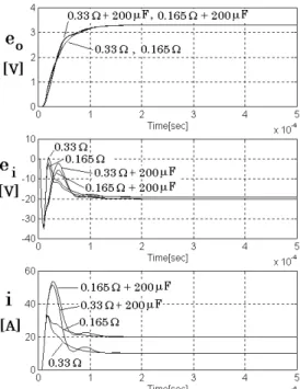
The simulation results of the startup responses are shown in Fig.8. From the output voltage y = eoin this figure, it turns out that the specifications are satisfied. It is checked that almost the same simulation results as Fig.8 are obtained when the input voltage Viis changed by±20%. The simula-tion result of the dynamic load responses is shown in Fig.9. Fig.9 is the result at resistive load and the value is changed as RL= 0.33↔ 0.165[Ω]. It is checked that almost the same simulation result as Fig.9 is obtained at parallel load of resis-tance (RL= 0.33↔ 0.165[Ω]) and capacity (CL= 200[µF]). It turns out that all the specifications are satisfied.
Experimental results when realizing the digital controller with the parameters of eq.(32) by using the DSP, and con-necting to the controlled object of eq.(1) are shown in Figs.10-15. Fig.10 and Fig.11 show startup responses at re-sisitive loads RL= 0.33[Ω] and RL= 0.165[Ω], respectively. Fig.12 shows a startup response at parallel load of resistance RL = 0.33[Ω] and capacity CL = 200[µF]. Fig.13 shows a startup response at parallel load of resistance RL= 0.165[Ω] and capacity CL = 200[µF]. From y = eo in these figure, it turns out that almost the same exprimental results as the simulation ones in Fig.8 are obtained and the specifications
Fig. 12. Experimental startup response at parallel load of RL= 0.33[Ω]) and CL= 200[µF]
Fig. 13. Experimental startup response at parallel load of RL= 0.165[Ω]) and CL= 200[µF]
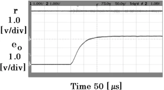
are satisfied. Fig.14 shows a startup responseare at resisitive load RL= 0.33[Ω] when the input voltages are 58[V]. It is checked that almost the same exprimental result is obtained at resisitive load RL = 0.33[Ω] when the input voltage is 38[V] It turns out that the specifications are satisfied when the input voltage Viis changed by±20%. Fig.15 shows a dy-namic load response at resistive load and the value changed as RL= 0.33↔ 0.165[Ω]. It turns out tha almost the same exprimental results as the simulation results in Fig.9 are ob-tained. It is checked that almost the same exprimental re-sults as Fig.15 are obtained at the parallel load of resistance (RL = 0.33↔ 0.165[Ω]) and capacity (CL= 200[µF]). Al-though load current(iL) changed suddenly from 20 [A] to 10 [A] or reverse, output voltage change is very small and is suppressed within about 50[mV]. It turns out that all the specification are satisfied.
5. Conclusion
In this paper, the concept for controller of DC-DC con-verter to attain the good robustness against an extensive load changes and input voltage change was given. The proposed digital controller was implemented on the DSP connecting to the controlled object. It was shown from some simulations and experiments that a sufficiently robust digital controller is realizable. The characteristics of the startup transient re-sponse and the dynamic load rere-sponse were improved by us-ing the proposed good approximate 2DOF digital controller. A control algorithm has been implemented with a short sam-pling time using DSP. This fact demonstrates the usefulness and practicality of our method. The future work is
experi-Fig. 14. Experimental result of a startup response at re-sisitive load (RL= 0.33[Ω]) when the input voltage is 58[V]
Fig. 15. Experimental dynamic load response at RL = 0.33↔ 0.165[Ω]
mental studies on a sudden change of the input voltage.
References
[1] L. Guo, J. Y. Hung, and R. M. Nelms, ”Digital con-troller Design for Buck and Boost Converters Using Root Locus”, IEEE IECON’2003, 1864/1869 (2003). [2] H. Guo, Y. Shiroishi and O. Ichinokura, ”Digital PI
Controller for High Frequency Switching DC/DC Con-verters Based on FPGA”, IEEE INTELEC’03, 536/541 (2003).
[3] K. Higuchi,K. Nakano, K. Araki and F. Chino, ”NEW ROBUST CONTROL OF PWM POWER AMPI-FIER,” IFAC 15th Triennial World Congress,(CD-ROM)(2002).
[4] K. Higuchi, K. Nakano, K. Araki and F. Chino, ”Robust Control of PWM Power Amplifier by Approximate 2-Degree-of-Freedom Digital Controller with Bumpless Mode Switching”, IEEE IECON’2003, 1835/1840(2003).
[5] K. Higuchi, K. Nakano, T.Kajikawa, E.Takegami, S.Tomioka, K.Watanabe, ”Robust Control of DC-DC Converter by High-Order Approximate 2-Degree-of-Freedom Digital Controller”, IEEE IECON’2004, (CD-ROM), 2004.
[6] H. Fukuda and M. Nakaoka, ”State-Vector Feed-back Controlled-based 100kHz Carrier PWM Power Conditioning Amplifier and Its High-Precision Current-Tracking Scheme”, IEEE IECON’93, pp. 1105/1110(1993).
![Fig. 14. Experimental result of a startup response at re- re-sisitive load (R L = 0.33[Ω]) when the input voltage is 58[V]](https://thumb-ap.123doks.com/thumbv2/123dokinfo/4891875.37143/6.892.463.789.372.560/fig-experimental-result-startup-response-sisitive-input-voltage.webp)
