www.nature.com/scientificreports
Reconfigurable Yagi-Uda antenna
based on a silicon reflector with a
solid-state plasma
Da-Jin Kim
1, Jang-Soon Park
2, Cheol Ho Kim
3, Jae Hur
1, Choong-Ki Kim
1, Young-Kyun Cho
3,
Jun-Bong Ko
2, Bonghyuk Park
3, Dongho Kim
2& Yang-Kyu Choi
1This paper describes the fabrication and characterization of a reconfigurable Yagi-Uda antenna based on a silicon reflector with a solid-state plasma. The silicon reflector, composed of serially connected p-i-n diodes, forms a highly dense solid-state plasma by injecting electrons and holes into the intrinsic region. When this plasma silicon reflector is turned on, the front-realized gain of the antenna increases by more than 2 dBi beyond 5.3 GHz. To achieve the large gain increment, the structure of the antenna is carefully designed with the aid of semiconductor device simulation and antenna simulation. By using an aluminum nitride (AlN) substrate with high thermal conductivity, self-heating effects from the high forward current in the p-i-n diode are efficiently suppressed. By comparing the antenna simulation data and the measurement data, we estimated the conductivity of the plasma silicon reflector in the on-state to be between 104 and 105 S/m. With these figures, silicon material with its technology is an
attractive tunable material for a reconfigurable antenna, which has attracted substantial interest from many areas, such as internet of things (IoT) applications, wireless network security, cognitive radio, and mobile and satellite communications as well as from multiple-input-multiple-output (MIMO) systems.
Recently, a reconfigurable antenna (RA) has received substantial interest from many areas, such as internet of things (IoT) applications, wireless network security, cognitive radio, and mobile and satellite communications as well as from multiple-input-multiple-output (MIMO) systems1–7. These areas need various types of
anten-nas with different radiation patterns, polarization, bandwidth, or operating frequencies to efficiently cope with numerous commercial services8. However, inserting multiple antennas into a single device is challenging because
of the limited space and high cost. In that respect, a reconfigurable antenna that can replace multiple antennas is very attractive in those areas. There are many different forms of reconfigurable antenna, such as an antenna using a varactor, a micro-electro-mechanical systems (MEMS) switch, a reconfigurable feeding network, an array structure, or tunable material9–13. Among them, tunable material has a big potential applicability because antenna
properties can be changed in many different ways: for example, selection of the material as a reflector, control of the length in the radiation part, and modification of the geometry of the antenna.
An example of the reconfigurable antenna using a tunable material is a plasma antenna. In a gas-phase plasma antenna, an ionized gas plasma formed in a discharge tube by bursts of applied RF power is used as an alterna-tive to metal conductors14,15. By turning on and off the plasma, the antenna is dynamically reconfigured without
the aid of RF elements. The plasma antenna also has a stealth property in the off-state because the antenna is reverted to a dielectric-phase, which is invisible to the radar16. In a solid-state plasma antenna, known as a plasma
silicon antenna, a cloud of electrons and holes replaces the metal conductors17. The density of the electron-hole
plasma can be controlled by light illumination, thermal heating, and voltage biasing with a wide range18–22. Hence,
conductivity (σsi) of the silicon can be intentionally modulated. It is inferred that the silicon provides superior
tunability to the plasma antenna by providing the electron-hole plasma with a high density23,24. Compared to
the gas-phase plasma antenna, the plasma silicon antenna has advantages in price and size. By employment of matured and commercial silicon-based fabrication technology, a confined area of the solid-state plasma with a
1School of Electrical Engineering, Korea Advanced Institute of Science and Technology, (KAIST) 291 Daehak-ro, Yuseong-gu, Daejeon, 34141, Republic of Korea. 2Deparment of Electrical Engineering, Sejong University, 209 Neungdong-ro, Seoul, 05006, Republic of Korea. 3Mobile RF Research Section, Electronics and Telecommunications Research Institute, 218 Gajeong-ro, Yuseong-gu, Daejeon, 34129, Republic of Korea. Da-Jin Kim, Jang-Soon Park and Cheol Ho Kim contributed equally to this work. Correspondence and requests for materials should be addressed to D.K. (email: [email protected]) or Y.-K.C. (email: [email protected])
Received: 6 September 2017 Accepted: 22 November 2017 Published: xx xx xxxx
www.nature.com/scientificreports/
tunable σsi can be precisely controlled with the aid of photolithography and ion implant. Moreover, the silicon
technology has the potential to provide low cost and mass production with high packing density by integrating DC-bias lines, RF-feed, and the control circuit with the plasma silicon antenna.
Herein, to verify silicon as a tunable material for a reconfigurable antenna, we selected the structure of a commonly used Yagi-Uda antenna for its simple structure and high gain25. The Yagi-Uda antenna is a directional
antenna composed of a simple driving element, a reflector, and directors26. High gain in a specific direction,
which is a measure of the amount of electromagnetic (EM) energy received in the specified direction, is required in numerous practical applications27–31. The reflector enhances the gain by reflecting the radiated wave toward
the forward direction while preventing backward radiation. If the reflector is replaced by silicon with high tun-ability of σsi, the antenna gain is accordingly modulated. Therefore, the Yagi-Uda antenna using a silicon-based
reflector is a simple and effective structure to demonstrate reconfigurability of the antenna. In our previous study, the feasibility of a primitive Yagi-Uda antenna with a silicon-based reflector was preliminarily reported32. The
Yagi-Uda antenna was turned on and off by biasing the DC voltage. Although it showed a gain difference between the on-state and off-state of the silicon-based reflector, it suffered from a small gain difference as well as a burning issue arising from a poor σsi, the self-heating effect, and radiation interference among adjacent DC-bias lines.
In this paper, we demonstrate a revamped reconfigurable Yagi-Uda antenna using a plasma silicon reflector for resolving the abovementioned problems and optimizing the antenna. We provide a guideline for designing the reconfigurable Yagi-Uda antenna with the plasma silicon reflector with the aid of numerical simulations, electromagnetic (EM) analysis, and experiments. A ceramic and polymer based printed circuit board (PCB) called the RF-35 substrate, which has been widely and commercially used, was replaced with an aluminum nitride (AlN) substrate that created heat-sink mitigating self-heating effects owing to its high thermal conductivity33.
The size of the antenna is also reduced due to the high permittivity (εAlN = 8.56 ε0) of the substrate. Prior to
fab-ricating the Yagi-Uda antenna, we optimized its structural parameters by combining the simulation data from the semiconductor device simulator (SILVACO)34 and from the antenna simulator (Ansys HFSS software)35 to
minimize the power consumption and interference among adjacent DC-bias lines. The reflector in the Yagi-Uda antenna was comprised of serially connected p-i-n diodes (diode with a wide intrinsic (i) semiconductor region between a p-type doped region (p) and a n-type doped region(n)), which could be turned on and off to control
σsi of the reflector. By analyzing the antenna reflection coefficients and radiation properties, we experimentally
demonstrated that the plasma silicon reflector was successfully tunable from an insulator to metal and vice versa. To the best of our knowledge, our group showed the measured gain of the fabricated plasma silicon antenna for the first time in our previous research. Herein, we demonstrate the full-functionality of the fabricated plasma sil-icon antenna, which includes both electrical properties of the p-i-n diode and the measured as well as simulated antenna characteristics.
Results and Discussion
A conceptual operation of the proposed reconfigurable Yagi-Uda antenna is shown in Fig. 1. The overall geome-try of the proposed reconfigurable Yagi-Uda antenna with a reconfigurable plasma silicon reflector, a monopole feeder, and three directors is shown in Fig. 1(a). A commercial AlN substrate with a dielectric constant of 8.56
Figure 1. (a) The geometry and (b) operational principle of the proposed reconfigurable Yagi-Uda antenna
using the plasma silicon reflector. (c) Conceptual 3-dimensional (3D) radiation patterns of the proposed antenna when the plasma silicon reflector is in the off-state or on-state.
www.nature.com/scientificreports/
has been chosen for its high thermal conductivity to efficiently dissipate heat generated from the plasma silicon reflector.
The operational principle of the proposed reconfigurable Yagi-Uda antenna is illustrated in Fig. 1(b). To obtain high antenna gain in the targeted positive z-direction, the wave reflected by the reflector must interfere construc-tively with the wave launching from the monopole driven element. In other words, they must be in the same phase at the position of the driven element, which is formulated by
l N
2 2 (1)
R
ϕ − β = π
where ϕR is the reflection phase of the reflected wave, β is the effective phase constant, and N is a positive integer.
Here, −2βl denotes the overall phase delay for the round-trip distance of 2l. The reflected wave is affected by the conductivity of the reflector, σsi. A higher σsi provides a stronger reflection, which is desirable for obtaining a
high gain in the positive z-direction. When the plasma silicon reflector is in the on-state, the antenna gain, which strongly depends on σsi, drastically increases. For easier understanding of the role of the reflector, conceptual
3-dimensional (3D) radiation patterns of the proposed antenna are shown in Fig. 1(c). To emphasize the effect of the reflector, these patterns are trimmed based on the result of the antenna simulation (refer to Supplementary Information S1). From these data, the influence of the reflector on the radiation property of the antenna is clearly confirmed.
One of the distinct features of the proposed Yagi-Uda antenna compared to a conventional Yagi-Uda antenna is that the reflector is fabricated using commercial silicon technology. To reflect the wave launched from the driven element, the reflector should have a σsi as high as possible. Herein, to achieve a high σsi, serially connected
p-i-n diodes are adopted. The σsi of intrinsic region in the p-i-n diode can be controlled by injection of electrons
and holes from the n-type and p-type heavily doped region to the intrinsic region by applying forward voltage between the p-type region and the n-type region. As shown in Fig. 2(c), serially connected p-i-n didoes are divided into several segments to control the operation voltage. Each segment shares the same operation voltage with the ground voltage of an adjacent segment. In other words, segments are connected in parallel, and the source of leakage current is inherently removed without use of any isolation technology, such as local oxidation of silicon (LOCOS) or shallow trench isolation. The fabrication process of the unit p-i-n diode is described in Fig. 2(a). First, to make the SOI wafer, one intrinsic wafer was bonded to another intrinsic wafer with a 1-μm oxide layer on the top, which is called buried oxide. It is desirable to have a top silicon wafer with its doping level as low as possible because a low doping level in the intrinsic region produces both a low σsi in the off-state
and a longer lifetime for carriers owing to a lower recombination rate36. Next, the top silicon of the bonded SOI
wafer was ground to a thickness of 5 μm. When the thickness of the top silicon (Tsi) is thinner than 5 μm, poor
uniformity of the top silicon arises from the limitation of the chemical mechanical polishing (CMP) process, which affects the device yield. Since a thickness of 5 μm is enough to reflect the incident wave, we can minimize the operating power (refer to Supplementary Information S2). In addition, the bottom silicon should be intrin-sic silicon and have a σsi lower than 0.01 S/m. Otherwise, the portion of incident wave is always reflected by the Figure 2. (a) The fabrication process of the unit p-i-n diode. (b) The optical photograph of the fabricated
p-i-n diode array. (c) The structure of serially connected p-i-n diodes, and the bias configuration of the array of diodes used to construct the plasma silicon reflector.
www.nature.com/scientificreports/
bottom silicon (refer to Supplementary Information S3). Then, the LOCOS process was conducted to isolate the active area from the dummy area. Afterwards, a highly n-typed doped (n+) junction was formed by
phospho-rus implantation with energy of 80 keV and a dose of 1016 cm−2. To make the junction deep, a drive-in process
was carried out. Similarly, after the highly p-typed doped (p+) junction was formed by boron implantation with
energy of 80 keV and a dose of 1016 cm−2, the drive-in process was applied once again. Two drive-in processes are
designed to make the p-type junction depth and the n-type junction depth the same: 1 μm. In the next step, tetra-ethyl orthosilicate (TEOS) was deposited by low-pressure chemical vapor deposition (LPCVD) to passivate the device and to make a via hole before metal deposition. Finally, forming gas annealing (FGA)37,38 was conducted
to passivate the interface between the TEOS and top silicon after the aluminum deposition via the sputtering process. An optical photograph of the completed plasma silicon reflector is shown in Fig. 2(b). After that, the bottom silicon of the fabricated plasma silicon reflector was ground to 63 μm to make the positon of the reflector comparable to the driven element before it was attached to the AlN substrate. Finally, the implanted bias lines on the substrate were connected to the metal pad of the plasma silicon reflector with gold wires.
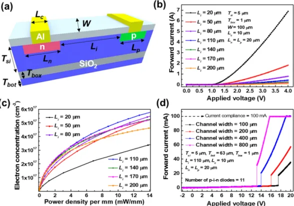
In the plasma silicon reflector, there are many device parameters to be optimized as shown in Fig. 3(a). We carefully conducted numerical simulations to optimize those parameters with the aid of the SILVACO Atlas. The contact length (Lc), the thickness of the buried oxide (Tbox), the length of the p-typed heavily doped region
(Lp), and the length of the n-type heavily doped region (Ln) are insensitive process parameters, which do not
significantly affect the electrical characteristic when they are large enough. Therefore, they were fixed as follows:
Lc is 10 μm, Tbox is 1 μm, and both Lp and Ln are 20 μm. However, the intrinsic channel length (Li) and Tsi are key
parameters that notably influence the reflector characteristics. Figure 3(b) shows the forward current versus the applied voltage characteristics of a unit p-i-n diode according to the Li. Below an applied voltage of 0.7 V, the
forward currents with various Li are similar, but beyond an applied voltage of 0.7 V, the p-i-n diode with a lower
Li exhibits a higher forward current due to a limited diffusion length and a decreased channel resistance39. From
the measured current, the electron concertation, which is proportional to σsi, is extracted according to the applied
voltage for each Li. Consideration of the electron concentration solely is enough to characterize σsi of the p-i-n
diode because the hole concentration is the same as the electron concentration with the opposite polarity. The dif-ference between electrons and holes is that electrons are injected from the n-type heavily doped region and holes are injected from the p-type heavily doped region. From the electron concertation versus applied voltage curves and I-V curves of the p-i-n diode, the change in the electron concentration according to the power density (mW/ mm) for each Li was calculated as shown in Fig. 3(c). The p-i-n diode shows semi-metallic characteristics with a
power consumption of a few milliwatts per millimeter. Since a Li of 110 μm has the highest electron concentration
at the given power density, Li was fixed at 110 μm. Measured I-V characteristics from a single segment, which is
composed of 11 p-i-n diodes, are shown in Fig. 3(d). Beyond the latch-up voltage, the forward current is abruptly
Figure 3. The measured and simulated electrical characteristics of the plasma silicon reflector (a) The geometry
of the structural parameters in the unit p-i-n diode. (b) Simulated I-V curves of the unit p-i-n diode according to Li. (c) Simulated curves of the electron concentration versus the power density according to Li. (d) Measured
www.nature.com/scientificreports/
increased because all the p-i-n diodes are turned on simultaneously40. This latch-up behavior is useful for the
selection of the appropriate operation voltage. σsi dramatically changes above the latch-up voltage. The
appro-priate operation voltage of the plasma silicon reflector during the antenna measurement in an anechoic chamber was set at 16 V with the consideration of the latch-up voltage. The channel width (W) of the p-i-n diode varied from 100 μm, 200 μm, and 400 μm to 800 μm. The forward current was linearly proportional to W. To increase the antenna gain, a wider W was preferred (refer to Supplementary Information S4). Finally, the optimized device parameters were Tsi of 5 μm, Li of 110μm, and W of 800 μm.
The cross-sectional view of the plasma silicon reflector is shown in Fig. 4(a). To design the antenna precisely, the actual distribution of carrier concertation in the channel region in the on-state should carefully be considered in antenna simulation. Therefore, the carrier concentration along the vertical direction and the lateral direction of the intrinsic region in the on-state was investigated through numerical simulation (refer to Supplementary Information S5). The carrier concentration of 5 × 1017 cm−3 was uniformly distributed along the vertical
direc-tion at a Li of 110 μm. The carrier concentration of 5 × 1017 cm−3 was also almost uniformly distributed along the
lateral direction at the same Li of 110 μm.
The overall shape of the fabricated antenna is shown in Fig. 4(b), which consists of a driving monopole antenna, 3 directors, the plasma silicon reflector, a microstrip transmission line, and 11 DC-bias lines. All metal patterns: the monopole antenna, the directors, the micro strip transmission line, and the DC-bias lines, were patterned by industrial silk screen printing41. Due to an adhesion problem, the metal patterns were composed
of gold/nickel/silver on a 1-mm-thick commercial AlN substrate, which served as the heat sink. The micro strip transmission line was connected to a 50 Ω coaxial cable. To evaluate the antenna characteristics of the fabricated antenna, the antenna input reflection coefficient (S11) and the antenna realized gain (antenna gain including the
amount of the EM energy loss reflected back to the source due to the impedance mismatch at the input port of the antenna) were primarily characterized. Supportive simulations were carried out for a study of the impedance matching property according to σsi, as shown in Fig. 4(c). From this, it is inferred that S11 is insensitive to σsi.
When σsi increased from 104 to 105 S/m, the impedance matching bandwidth in which S11 was lower than −10 dB,
also widened approximately from 450 MHz to 550 MHz, which corresponded to a fractional bandwidth of 8.86% and 11.16%. The simulated realized gain in the positive z-direction according to σsi is also displayed in Fig. 4(d).
The realized gain is proportional to σsi, which is far more sensitive to σsi than S11.
The measured antenna characteristics: S11 and radiation properties, are presented in Fig. 5, which reveals that
the impedance matching bandwidth is approximately 1.5 GHz covering from 4.5 to 6 GHz, which corresponds to a fractional bandwidth of 28.57%.
The measurement environment is described in Fig. 5(b). Both the receiver and the Yagi-Uda antenna are located in an anechoic chamber whose inner wall is composed of the absorber. Figure 5(c) shows how the realized gain in the positive z-direction varies when the plasma silicon reflector is turned on and off. When the plasma silicon reflector is turned on, the realized gain increases more than 2 dBi beyond 5.3 GHz. At 5.1 GHz, the realized gain is higher in the off-state, which might be due to the many gold wires connecting the plasma silicon reflector to the DC-bias lines (refer to Supplementary Information S6). Comparing resonant frequencies in Figs 4(c) and
5(a) reveals that the measured S11 has shifted up about 400 MHz toward the high frequency region. A similar Figure 4. (a) The cross-sectional view of the simulated antenna. (b) The simulated S11 according to σsi. (c) The
www.nature.com/scientificreports/
frequency shift can also be found from the realized gain behaviors shown in Figs 4(d) and 5(c). From the realized gain shift, it is important to notice that σsi can be estimated as between 104 and 105 S/m. The radiation pattern on
an E-plane containing a radiating electric field vector, which was measured at 5.3 GHz is shown in Fig. 5(d). As the plasma silicon reflector is turned on, the front-realized gain (at 0°) increases and the rear-realized gain (at 180°) decreases, which proves the proposed silicon reflector well mimics a metallic conductor.
In our study, the silicon technology was used to make the Yagi-Uda antenna reconfigurable. The silicon mate-rial exhibited good tunability by forming a highly dense solid-state plasma in the intrinsic channel region of the p-i-n diode. When the plasma silicon reflector was in the on-state, the realized gain in the positive z-direction increased more than 2 dBi beyond 5.3 Ghz compared to the off-state. A large gain increment was achieved by structure optimization with the device and antenna simulator and self-heating relaxation with the AlN substrate. From measuring the characteristic of the fabricated Yagi-Uda antenna in an anechoic chamber, we estimated the
σsi in the on-state to be between 104 and 105 S/m. This paper is the first to demonstrate full-functionality of the
plasma silicon antenna, which includes the properties of the silicon device and the measured characteristics of the fabricated antenna. Our results confirm that the silicon material with its technology has a potential to be directly applied to a reconfigurable antenna as a radiating element or entire antennas in the future.
Methods
Fabrication of the antenna.
The SOI wafer was fabricated by a commercial wafer bonding technology. Forming p-i-n diodes on the SOI wafer was conducted through a commercial service of silicon technology. The Yagi-Uda antenna was fabricated on the AlN substrate with metal patterns made by industrial silk screen printing. (Y.TECH, Co.) Rn2 technologies, Co. provided the AlN substrate. By silk screen printing, a silver layer with a thick-ness of 8 μm was deposited and patterned on the AlN substrate. Solider resistor was also deposited on the silver pat-terns. The electroless plating was conducted to deposit a nickel layer with a thickness of 3 μm and a gold layer with a thickness of 0.1~0.2 μm. All interconnections were carried out by the commercial company. (RUATECH Inc.).Characterization.
All electrical measurements were carried out without any device encapsulation. Electrical measurements were carried out using a HP4156 semiconductor parameter analyzer under ambient conditions. The antenna input reflection coefficient (S11) was measured by Vector Network Analyzer ZNB40 (Rohde &Schwarz GmbH). The antenna realized gain was measured by the antenna measurement system with a full ane-choic chamber in IoT center, Incheon, South Korea. The antenna measurement system includes PNA network analyzer E8362B (Agilent Technologies, Inc), microwave system amplifier 83017A (Keysight Technologies, Inc), and power supply 87421A (Keysight Technologies, Inc). Gain-transfer method was used.
Figure 5. The effect of switching states on the proposed plasma silicon reflector (a) S11. (b) The gain in the
positive z-direction. (c) 2-dimenstional (2D) radiation patterns at 5.3 GHz. (d) A photograph of a fully anechoic chamber with the receiving horn antenna and the fabricated Yagi-Uda antenna on a commercial rohacell holder.
www.nature.com/scientificreports/
References
1. Kgwadi, M. & Drysdale, T. D. Diode-switched thermal-transfer printed antenna on flexible substrate. Electronics Letters 52, 258–260,
https://doi.org/10.1049/el.2015.3060 (2016).
2. Valliappan, N., Lozano, A. & Heath, R. W. Antenna Subset Modulation for Secure Millimeter-Wave Wireless Communication. IEEE
Transactions on Communications 61, 3231–3245, https://doi.org/10.1109/TCOMM.2013.061013.120459 (2013).
3. Mookiah, P. & Dandekar, K. R. Enhancing wireless security through reconfigurable antennas. In 2010 IEEE Radio and Wireless
Symposium (RWS), New Orleans, LA, USA, 593–596, https://doi.org/10.1109/RWS.2010.5434129 (2010).
4. Tawk, Y. & Christodoulou, C. G. A New Reconfigurable Antenna Design for Cognitive Radio. IEEE Antennas and Wireless
Propagation Letters 8, 1378–1381, https://doi.org/10.1109/LAWP.2009.2039461 (2009).
5. Mak, A. C. K., Rowell, C. R., Murch, R. D. & Mak, C. L. Reconfigurable Multiband Antenna Designs for Wireless Communication Devices. IEEE Transactions on Antennas and Propagation 55, 1919–1928, https://doi.org/10.1109/TAP.2007.895634 (2007). 6. Christodoulou, C. G., Tawk, Y., Lane, S. A. & Erwin, S. R. Reconfigurable Antennas for Wireless and Space Applications. Proceedings
of the IEEE 100, 2250–2261, https://doi.org/10.1109/JPROC.2012.2188249 (2012).
7. Piazza, D., Kirsch, N. J., Forenza, A., Heath, R. W. & Dandekar, K. R. Design and Evaluation of a Reconfigurable Antenna Array for MIMO Systems. IEEE Transactions on Antennas and Propagation 56, 869–881, https://doi.org/10.1109/TAP.2008.916908 (2008). 8. Jennifer, T. B. Reconfigurable Antennas. (Morgan & Claypool, 2007).
9. Behdad, N. & Sarabandi, K. Dual-band reconfigurable antenna with a very wide tunability range. IEEE Transactions on Antennas
and Propagation 54, 409–416, https://doi.org/10.1109/TAP.2005.863412 (2006).
10. Weedon, W. H., Payne, W. J. & Rebeiz, G. M. MEMS-switched reconfigurable antennas. IEEE Antennas and Propagation Society
International Symposium. 2001 Digest. Held in conjunction with: USNC/URSI National Radio Science Meeting (Cat. No.01CH37229), Boston, MA, USA, 8-13 July 2001 653, 654–657, https://doi.org/10.1109/APS.2001.960181 (2001).
11. Row, J. S. & Hou, M. J. Design of Polarization Diversity Patch Antenna Based on a Compact Reconfigurable Feeding Network. IEEE
Transactions on Antennas and Propagation 62, 5349–5352, https://doi.org/10.1109/TAP.2014.2341271 (2014).
12. Tomasic, B. et al. The geodesic dome phased array antenna for satellite control and communication - subarray desing, development and demonstration. In IEEE International Symposium on Phased Array Systems and Technology, Boston, MA, USA, 14–17 Oct. 411–416, https://doi.org/10.1109/PAST.2003.1257017 (2003).
13. Pozar, D. M. & Sanchez, V. Magnetic tuning of a microstrip antenna on a ferrite substrate. Electronics Letters 24, 729–731, https:// doi.org/10.1049/el:19880491 (1988).
14. Kumar, R. & Bora, D. A reconfigurable plasma antenna. Journal of Applied Physics 107, 053303, https://doi.org/10.1063/1.3318495
(2010).
15. Borg, G. G., Harris, J. H., Miljak, D. G. & Martin, N. M. Application of plasma columns to radiofrequency antennas. Applied Physics
Letters 74, 3272–3274, https://doi.org/10.1063/1.123317 (1999).
16. Alexeff, I. et al. Experimental and theoretical results with plasma antennas. IEEE Transactions on Plasma Science 34, 166–172,
https://doi.org/10.1109/TPS.2006.872180 (2006).
17. Fathy, A. E. et al. Silicon-based reconfigurable antennas-concepts, analysis, implementation, and feasibility. IEEE Transactions on
Microwave Theory and Techniques 51, 1650–1661, https://doi.org/10.1109/TMTT.2003.812559 (2003).
18. Levinshtein, M., Rumyantsev, S. & Shur, M. Handbook Series on Semiconductor Parameters: In 2 Volumes. (World Scientific, 1996). 19. Panagamuwa, C. J., Chauraya, A. & Vardaxoglou, J. C. Frequency and beam reconfigurable antenna using photoconducting switches.
IEEE Transactions on Antennas and Propagation 54, 449–454, https://doi.org/10.1109/TAP.2005.863393 (2006).
20. Chang, B. C. C., Qian, Y. & Itoh, T. A reconfigurable leaky mode/patch antenna controlled by PIN diode switches. In IEEE Antennas
and Propagation Society International Symposium. 1999 Digest. Held in conjunction with: USNC/URSI National Radio Science Meeting
(Cat. No.99CH37010), Orlando, FL, USA, 11–16 July 2694, 2694–2697, https://doi.org/10.1109/APS.1999.789363 (1999). 21. Yashchyshyn, Y., Derzakowski, K., Bajurko, P. R., Marczewski, J. & Kozłowski, S. Time-Modulated Reconfigurable Antenna Based
on Integrated S-PIN Diodes for mm-Wave Communication Systems. IEEE Transactions on Antennas and Propagation 63, 4121–4131, https://doi.org/10.1109/TAP.2015.2444425 (2015).
22. Ma, C. L. & Lauritzen, P. O. A simple power diode model with forward and reverse recovery. IEEE Transactions on Power Electronics
8, 342–346, https://doi.org/10.1109/63.261002 (1993).
23. Jackson, R. P., Mitchell, S. J. N. & Fusco, V. Physical modeling of millimetre wave signal reflection from forward biased PIN diodes.
Solid-State Electronics 54, 149–152, https://doi.org/10.1016/j.sse.2009.12.009 (2010).
24. Zhai, Y. et al. Simulation and structure analysis of reconfigurable solid plasma channel based on SPINs. Microelectronic Engineering
145, 49–52, https://doi.org/10.1016/j.mee.2015.03.003 (2015).
25. Cai, Y., Guo, Y. J. & Bird, T. S. A Frequency Reconfigurable Printed Yagi-Uda Dipole Antenna for Cognitive Radio Applications.
IEEE Transactions on Antennas and Propagation 60, 2905–2912, https://doi.org/10.1109/TAP.2012.2194654 (2012). 26. Balanis, C. A. Antenna Theory: Analysis and Design. (Wiley, 2015).
27. DeJean, G. R. & Tentzeris, M. M. A New High-Gain Microstrip Yagi Array Antenna With a High Front-to-Back (F/B) Ratio for WLAN and Millimeter-Wave Applications. IEEE Transactions on Antennas and Propagation 55, 298–304, https://doi.org/10.1109/ TAP.2006.889818 (2007).
28. Mobashsher, A. T., Islam, M. T. & Misran, N. A Novel High-Gain Dual-Band Antenna for RFID Reader Applications. IEEE Antennas
and Wireless Propagation Letters 9, 653–656, https://doi.org/10.1109/LAWP.2010.2055818 (2010).
29. Huang, J. & Densmore, A. C. Microstrip Yagi array antenna for mobile satellite vehicle application. IEEE Transactions on Antennas
and Propagation 39, 1024–1030, https://doi.org/10.1109/8.86924 (1991).
30. Feresidis, A. P. & Vardaxoglou, J. C. High gain planar antenna using optimised partially reflective surfaces. IEE Proceedings -
Microwaves, Antennas and Propagation 148, 345–350, doi:https://doi.org/10.1049/ip-map:20010828 (2001).
31. Arnieri, E., Boccia, L., Amendola, G. & Massa, G. D. A Compact High Gain Antenna for Small Satellite Applications. IEEE
Transactions on Antennas and Propagation 55, 277–282, https://doi.org/10.1109/TAP.2006.889831 (2007).
32. Cho, Y. K., Kim, C. H., Hyun, S., Lee, K. C. & Park, B. H. Semiconductor-based reflector antenna using integrated PIN diodes. in
2016 International Symposium on Antennas and Propagation (ISAP), Okinawa, Japan, 24–28 Oct. 748–749 (2016).
33. Kurokawa, Y., Utsumi, K., Takamizawa, H., Kamata, T. & Noguchi, S. A1N Substrates with High Thermal Conductivity. IEEE
Transactions on Components, Hybrids, and Manufacturing Technology 8, 247–252, https://doi.org/10.1109/TCHMT.1985.1136500
(1985).
34. Manual, ATLAS User’S. “Device simulation software.” Silvaco Int., Santa Clara, CA (2008). 35. ANSYS HFSS [Online]. Available: http://www.ansys.com.
36. Fossum, J. G., Mertens, R. P., Lee, D. S. & Nijs, J. F. Carrier recombination and lifetime in highly doped silicon. Solid-State Electronics
26, 569–576, https://doi.org/10.1016/0038-1101(83)90173-9 (1983).
37. Sopori, B. L. et al. Hydrogen in silicon: A discussion of diffusion and passivation mechanisms. Solar Energy Materials and Solar Cells
41, 159–169, https://doi.org/10.1016/0927-0248(95)00098-4 (1996).
38. Cartier, E., Stathis, J. H. & Buchanan, D. A. Passivation and depassivation of silicon dangling bonds at the Si/SiO2 interface by atomic hydrogen. Applied Physics Letters 63, 1510–1512, https://doi.org/10.1063/1.110758 (1993).
39. Kim, D. J. et al. Optimization of the intrinsic length of a PIN diode for a reconfigurable antenna. In 2016 International Conference on
Electronics, Information, and Communications (ICEIC), Da Nang, Vietnam, 27–30 Jan. 1–4, https://doi.org/10.1109/ ELINFOCOM.2016.7562965 (2016).
www.nature.com/scientificreports/
40. Jae, H. et al. Silicon-Based Yagi-Uda Antenna Reflector, In 2017 International Conference on Electronics, Information, and
Communications (ICEIC), Phuket, Thailand, 11–14 Jan. 178–181 (2017).
41. Krebs, F. C., Alstrup, J., Spanggaard, H., Larsen, K. & Kold, E. Production of large-area polymer solar cells by industrial silk screen printing, lifetime considerations and lamination with polyethyleneterephthalate. Solar Energy Materials and Solar Cells 83, 293–300,
https://doi.org/10.1016/j.solmat.2004.02.031 (2004).
Acknowledgements
This work was supported by Institute for Information & communications Technology Promotion(IITP) grant funded by the Korea government(MSIT). (2015-0-00268, Development on Semi-conductor based Smart Antenna for Future Mobile Communications).
Author Contributions
D.-J. Kim, J.-S. Park, C.H. Kim, D. Kim., and Y.-K. Choi conceived the idea and designed the experiment. D.-J. Kim, J. Hur, and C.-K. Kim carried out fabrication of the silicon device. D.-J. Kim and J. Hur conducted the device simulation and measured the electrical characteristic of the fabricated silicon device. J.-S. Park, C.H. Kim, Y.-K. Cho, J.-B. Ko. and B. Park carried out fabrication of the antenna. C.H. Kim and Y.-K. Cho suggested the idea of using the AlN substrate. J.-S. Park and J.-B. Ko conducted the antenna simulation. J.-S. Park, D.-J. Kim, C.H. Kim, and Y.-K. Cho measured the antenna characteristics. D.-J. Kim, J.-S. Park, and D. Kim analyzed the experimental data. D.-J. Kim, J.-S. Park, C.H. Kim, D. Kim, and Y.-K. Choi prepared the manuscript.
Additional Information
Supplementary information accompanies this paper at https://doi.org/10.1038/s41598-017-17425-8.
Competing Interests: The authors declare that they have no competing interests.
Publisher's note: Springer Nature remains neutral with regard to jurisdictional claims in published maps and
institutional affiliations.
Open Access This article is licensed under a Creative Commons Attribution 4.0 International
License, which permits use, sharing, adaptation, distribution and reproduction in any medium or format, as long as you give appropriate credit to the original author(s) and the source, provide a link to the Cre-ative Commons license, and indicate if changes were made. The images or other third party material in this article are included in the article’s Creative Commons license, unless indicated otherwise in a credit line to the material. If material is not included in the article’s Creative Commons license and your intended use is not per-mitted by statutory regulation or exceeds the perper-mitted use, you will need to obtain permission directly from the copyright holder. To view a copy of this license, visit http://creativecommons.org/licenses/by/4.0/.