32-4 / Y. H. Hwang
• IMID 2009 DIGEST
Abstract
Thin-film transistors (TFTs) with an aluminum indium oxide (AIO) channel layer were fabricated via a simple and low-cost sol-gel process. Effects of annealing temperature and time were investigated for better TFT performance. The sol-gel AIO TFTs were annealed as low as 350℃. They exhibit n-type semiconductor behavior, a mobility higher than 19 cm2/V·s and an
on-to-off current ratio greater than 108.
1. Introduction
Transparent thin film transistors (TTFTs) including oxide active channel layer are of great current interest for transparent electronics such as flat panel displays, flexible displays, radio-frequency identification tags and smart windows [1, 2, 3]. In particular, not only the research field but also the industrial field have much interest in oxide TFTs after they are considered as a prominent candidate for the backplane of AMOLED and AMLCD [4].
Metal oxide semiconductors have many advantages such as transparency due to their large band gap, high uniformity for large size fabrication, environmental stability and high field-effect. Many transparent oxide semiconductors (TOSs) such as zinc oxide [5], zinc oxide [6], zinc-tin oxide [7], indium-gallium-zinc oxide [2], and indium oxide [8] have been reported for transparent channel layers in TTFTs. However, TOSs are generally prepared by vacuum-deposition methods such as rf magnetron sputtering and pulsed laser deposition which require high costs.
Solution processed thin film deposition such as a sol-gel method could offer many advantages such as simplicity, high throughput, and low-cost compared to vacuum-deposition process. In addition, it enables the direct patterning (i.e. inkjet printing and roll-to-roll process) that could replace the conventional photolithographic techniques.
2. Experimental
The metal precursor solution for the AIO channel layer was prepared by dissolving 0.1 M of indium acetate [In(C2H3O2)3, Aldrich] and aluminum
acetylacetonate [Al(C5H7O2)3, Aldrich] in
2-methoxyethanol [C3H8O2, Aldrich]. Amount of Al
precursor in the precursor solution was 40 % of indium precursor. In order to form a stable solution, the indium acetate precursor was chelated with 0.4 M of ethylenediamine (EDA, NH2CH2CH2NH2, Aldrich).
The solution was stirred at room temperature for half an hour to make a transparent and homogeneous solution. After sufficient reaction, the solution was filtered through a 0.22 ㎛ syringe filter (PTFE, GE)
and spin-coated at a speed of 5000rpm atop of the SiO2/Si substrate for 30 s. The 50W of oxygen plasma
treatment was applied for 5mins just before the spin-coating in order to remove unnecessary organics on the substrate using conventional plasma cleaner. A 100nm SiO2 layer, which served as a gate dielectric,
was thermally grown on the top of the heavily boron (p+) doped silicon wafer. After film deposition, it was annealed on a hot plate under air at various temperatures.
The structural and electrical properties of AIO thin films were characterized by using various analyzing tools. A thin film x-ray diffractometer (XRD, Rigaku) was used to investigate the crystallinity and crystal orientation of the film. The electrical property of AIO TFTs was analyzed by HP 4145B semiconductor parameter analyzer and probe station.
3. Results and discussion
Formation of metal oxide thin film relies heavily on annealing process in sol-gel method. In my previous work, decomposition behavior of AIO precursor solution was studied by thermogravimetric analysis (TGA, TA instrument Q50) [9]. According to the
Low Temperature Annealed Sol-Gel Aluminum Indium Oxide
Thin Film Transistors
Young Hwan Hwang, Jun Hyuck Jeon, Seok-Jun Seo, and Byeong-Soo Bae*
Dept. of Materials Science and Engineering, KAIST, Daejeon 305-701, Korea
Tel.:82-42-350-4119, E-mail: [email protected]
32-4 / Y. H. Hwang
IMID 2009 DIGEST •
result, annealing temperature was controlled to 300°C, 350°C, and 500°C for 1 hr. The transfer curves at a fixed VDS = 40 V, displayed in figure 1, show that
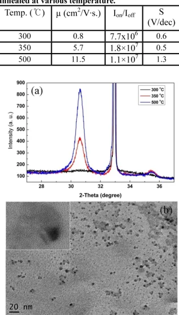
annealing temperature affects the electrical property of AIO TFTs clearly. As the annealing temperature increases on-current and off-current increase and transfer curves are shifted to negative voltage. The summarized electrical parameters are listed in the table 1. It is generally accepted that higher annealing temperature results in better crystallinity [10]. The better crystallinity of the film increases the carrier concentration, which is related to the shift of transfer curve, and improves electron conduction ability. The XRD patterns, shown in figure 2a, support the better crystallinity with higher annealing temperature. Clear current modulation behavior with gate bias is observed even at 300℃ annealed AIO TFT with
amorphous phase. Although the mobility is low, its sub-threshold swing and on-to-off current ratio are sufficient enough to drive the electronic circuits and its low annealing temperature shows the possibility of low temperature process. It is expected that 300 ℃
annealed AIO TFT would have a chance to find new applications such as e-paper or where low temperature process is necessary [11]. In addition, its low temperature processibility allows use of various substrates such as soda-lime glass and plastic substrates.
Fig. 1. Transfer characteristics for AIO TFTs with various annealing temperature for VDS = 40 V with structure of L=220 ㎛ and W=1000 ㎛.
The 500℃ annealed sample shows good electron
conduction property. It is generally accepted that high temperature annealing improves the crystallinity, defects level, and interface between semiconductor and gate dielectric of the films and results in better TFT performance. However, in this case, its
off-current and sub-threshold swing, that are related to defects and interface, are higher than 350℃ annealed
sample. The results indicate that too high temperature annealing (i.e., 500℃) deteriorates the quality of the
film and generates the defects in the film and oxygen vacancy on the surface of the film by breaking the bonding between indium and oxygen or evaporation of metal cations.
TABLE 1. Electrical properties of AIO TFTs annealed at various temperature.
Temp. (
℃) µ (cm
2/V·s.) I
on/I
offS
(V/dec)
300 0.87.7x10
6 0.6 350 5.71.8×10
7 0.5 500 11.51.1×10
7 1.3Fig. 2. (a) θ-2θ XRD analysis of AIO thin films with various annealing temperature on SiO2/Si substrate. (b) TEM surface image of AIO thin-film annealed at 350℃ for 1h and magnified image of
nano size crystal (inset).
Figure 2b shows the TEM surface image of AIO thin-film annealed at 350℃ for 1 hr. The image
32-4 / Y. H. Hwang
• IMID 2009 DIGEST
indicates that the film is partially crystallized. The size of crystallites are around 3-5nm and they are distributed over the film. The inset shows the magnified image of crystallite. The back part with grid is well crystallized section while white part is in amorphous phase.
Fig. 3. (a) Transfer characteristics for AIO TFTs with various annealing time for VDS = 40 V with structure of L=220 ㎛ and W=1000 ㎛. (b)
Output characteristics for the AIO TFT annealed at 350 for 2℃ hrs with various gate voltages.
Effects of annealing time of the AIO TFTs were displayed in figure 3a. The effects were quite clear at the early stage of variation (i.e. 1 hr and 2 hrs). However, any change in electrical property was not observed with the annealing time over 2 hrs. As the annealing time increases, the on-current and level of defects were improved and the transfer curve was shifted to negative voltage. The result indicates that longer annealing time elevates the performance of the TFTs in terms of mobility and sub-threshold swing which are related to faster and accurate operation of the devices.
Figure 3b shows the drain current versus drain-to-source voltage (ID-VDS) output characteristics of AIO
TFT, annealed at 350 ℃, for various gate voltages
(VG). Clear pinch-off and current saturation behaviors
are observed in output characteristics which are essential to adopt the conventional TFT theory to explain the operation of AIO TFTs [2]. As a result, it is natural to conclude that 350 ℃ is the suitable
annealing temperature for TFT application. The optimized AIO TFT exhibits channel mobility of µ =
19.6 cm2/V·s and shows n-type semiconductor
behavior with 350 ℃ annealing. The threshold
voltage is around 10V, sub-threshold swing is 0.5V/decade and on-to-off ratio is 1.7×10⁸ with low
off-current of 8.1×10⁻¹² which are compatible with the
results of vacuum processed oxide TFTs.
4. Summary
We have demonstrated highly transparent aluminum indium oxide thin film transistors with simple and low-cost spin coating process. It shows good electrical properties and operates in accumulation mode on a positive gate bias. Moreover, its low annealing temperature (350 °C) promises the use of various substrates (e.g. soda-lime glass and plastic substrates). These results reveal that the solution processed AIO TFT is the suitable device for high performance display back planes and transparent electronics.
Acknowledgement
This research was financially supported by the Ministry of Knowledge Economy (MKE) and the Korea Institute for Advancement of Technology (KIAT) through the Human Resource Training Project for Strategic Technology. This work was also supported by Basic Science Research Program through the National Research Foundation of Korea(NRF) funded by the Ministry of Education, Science and Technology (R11-2007-045-03002-0).
5. References
1. P. Gorrn, M. Sander, J. Meyer, M. Kroger, E. Becker, H. Johannes, W. Kowalsky, and T. Riedl, Adv. Mater. 18, p.738 (2006)
2. K. Nomura, H. Ohta, A. Takagi, T. Kamiya, M. Hirano, and H. Hosono, Nature 432, p.488 (2004). 3. V. Subramanian, J. M. J. Frechet, P. C. Channg, D.
32-4 / Y. H. Hwang
IMID 2009 DIGEST •
C. Huang, J. B. Lee, S. E. Molesa, A. R. Murphy, D. R. Redinger, and S. K. Volkman, Proceedings of the IEEE. 93, p.1330 (2005)
4. J. F. Wager, Science 300, p.1245 (2003).
5. R. L. Hoffman, B. J. Norris, and J. F. Wager, Appl. Phys. Lett. 82, p.733 (2003)
6. B. Yaglioglu, H. Y. Yeom, R. Beresford, and D. C. Paine, Appl. Phys. Lett. 89, p.062103 (2006)
7. H. Q. Chiang, J. F. Wager, R. L. Hoffman, J. Jeong, and D. A. Keszler, Appl. Phys. Lett. 86, p.013503
(2005)
8. L. Wang, M. Yoon, G. Lu, Y. Yang, A. Facchetti, and T. J. Marks, Nature mater. 5, p.893 (2006)
9. Y. H. Hwang, J. H. Jeon, S. Seo, and B. Bae,
Electrochem. Solid-State Lett.12, p.H336 (2009)
10. B. S. Ong, C. Li, Y. Li, Y. Wu, and R. Loutfy, J. Am. Chem. Soc. 129, p.2750 (2007)
11. E. Fortunato, N. Correia, P. Barquinha, L. Pereira, G. Goncalves, R. Martins, IEEE Electron Device Lett.29, p.988 (2008)