N A N O E X P R E S S
Open Access
Nanoscale observation of surface potential and
carrier transport in Cu
2
ZnSn(S,Se)
4
thin films
grown by sputtering-based two-step process
Gee Yeong Kim
1, Ju Ri Kim
1, William Jo
1*, Dae-Ho Son
2, Dae-Hwan Kim
2and Jin-Kyu Kang
2Abstract
Stacked precursors of Cu-Zn-Sn-S were grown by radio frequency sputtering and annealed in a furnace with Se metals to form thin-film solar cell materials of Cu2ZnSn(S,Se)4(CZTSSe). The samples have different absorber layer
thickness of 1 to 2μm and show conversion efficiencies up to 8.06%. Conductive atomic force microscopy and Kelvin probe force microscopy were used to explore the local electrical properties of the surface of CZTSSe thin films. The high-efficiency CZTSSe thin film exhibits significantly positive bending of surface potential around the grain boundaries. Dominant current paths along the grain boundaries are also observed. The surface electrical parameters of potential and current lead to potential solar cell applications using CZTSSe thin films, which may be an alternative choice of Cu(In,Ga)Se2.
Keywords: Cu2ZnSn(S,Se)4; Cu(In,Ga)Se2; Kesterite; Conductive atomic force microscopy; Kelvin probe
force microscopy
PACS number: 08.37.-d; 61.72.Mm; 71.35.-y Background
Cu2ZnSn(S,Se)4(CZTSSe) quaternary semiconductors
at-tract a lot of interest for thin-film solar cells [1]. Competi-tion in the solar cell market is nowadays hard-hitting, so it is getting more concern on the cost in the manufacturing of the thin-film solar cells. CZTSSe consists of relatively cheap and earth-abundant elements of Zn and Sn. In con-trast, Cu(In,Ga)Se2 (CIGS), which is now mostly
pro-mising for commercialization, has expensive and rare elements of In and Ga. CZTSSe shows high absorption coefficient and the band gap of it can be tuned with chan-ging S and Se composition.
So far, the highest conversion efficiency of CZTSSe is reported as 11.1% in non-vacuum process with hydra-zine [2] and 9.2% in vacuum process by co-evaporation [3,4]. Very recently, Solar Frontier announced the con-version efficiency of 10.8% in the CZTSSe solar cell module of 14 cm2 [5], which indicates presumably 12 to 13% of the conversion efficiency in the cell level. For large area deposition, sputtering methods have an
advantage in production of CZTS-based solar cells [6,7]. It is likely that compound sources such as ZnS and SnS can improve adhesion between the substrate and the thin film during deposition. Moreover, it is believed that the method can increase grain size, control composition, and improve surface morphology of precursors [8,9]. In order to put Se into the as-grown CZTS stacked cursors, optimization of annealing conditions of the pre-cursors in Se atmosphere is decisively important. In previous reports, the different stacking orders of precur-sors determine the crystallinity and grain growth of the CZTSSe thin films [10,11]. The results showed dense morphology and little voids on surface in case of Cu/ SnS/ZnS/Mo/glass [12,13].
There are some models to exhibit the advantageous properties of grain boundaries (GBs) of polycrystalline CIGS. Jiang et al. proposed that GBs acting as a factor to improve cell performance contrary to single-crystal solar cells by scanning probe characterization. GBs of CIGS drive majority carriers to repel out of the regime, which results in suppression of recombination [14,15]. Yan et al. suggested that GBs in CIGS electrically benign and not harmful to photovoltaic due to not creating deep levels
* Correspondence:[email protected]
1Department of Physics, Ewha Womans University, Seoul 120-750, Korea Full list of author information is available at the end of the article
© 2014 Kim et al.; licensee Springer. This is an Open Access article distributed under the terms of the Creative Commons Attribution License (http://creativecommons.org/licenses/by/2.0), which permits unrestricted use, distribution, and reproduction in any medium, provided the original work is properly cited.
[16]. On the other hand, valence band maximum at GBs acts as hole barriers, it reduces recombination at GBs [17]. Recently, Abou-Ras et al. identified Se-Se-terminated Σ3 {112} twin boundaries, indicating that Cu is depleted and In is enriched in the two atomic planes next to the twin boundary by high-resolution scanning transmission elec-tron microscopy and elecelec-tron energy-loss spectroscopy [18]. Takahashi group in Japan also reported that down-ward band bending of the conduction band and broaden-ing of the band gap near GBs are observed by photo-assisted Kelvin probe force microscopy. It accounts for photo-carriers well separate and suppress the recombin-ation at GBs [19]. Therefore, we have to investigate care-fully carrier transport at GB in CZTSSe thin films, which is not yet clearly identified for the role of GBs. We already reported positive potential bending of GBs on CZTSe thin films, grown by electron co-evaporation, which showed 2% to 3% of conversion efficiency [20]. In this study, we investigate sputtered CZTSSe thin-film solar cells, which exhibit better device performance than the previous sam-ples. We report local carrier transport and surface poten-tial of CZTSSe thin films using conductive atomic force microscopy (C-AFM) and Kelvin probe force microscopy (KPFM), respectively. For the complete understanding of the behaviors at GBs in CIGS films, recombination at GBs is diminished also due to downward band bending re-duced density of deep-level in-gap states (i.e., recombin-ation centers) and expect relatively efficient minority-carrier collection at GBs, as shown by scanning tunneling microscopy (STM) measurements [21,22]. Future analysis using STM can be addressed for GBs of CZTSSe thin films.
Method
CZTSSe thin films were grown on Mo-coated soda-lime glass substrates. The metal precursor layers were depos-ited by radio frequency sputtering using Cu, ZnS and SnS targets. The staking order of the precursors in this study was Cu/SnS/ZnS/Mo/glass. Thickness of each stacked layer was changed from 0.4 to 0.7μm. After the deposition, the precursors were annealed with Se metals in a furnace at 590°C for 20 min. Thickness of the annealed CZTSSe film was 1.8 μm for this study. From X-ray diffraction, the film shows single phase of CZTSSe without any significant second phases. We obtained the final composition is Cu/(Zn + Sn) ~ 0.94 and Zn/Sn ~ 1.65 of CZTSSe thin films by energy dispersive spec-trometry (EDS). S/Se ratio is estimated to be approxi-mately 0.1. The grain size indicates 1 to 2 μm of the CZTSSe thin film investigated by field emission scanning electron microscopy (FE-SEM) (JSM-700 F).
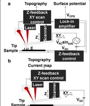
KPFM and C-AFM measurements were carried out using a commercial AFM (n-Tracer, Nanofocus Inc., Seoul, South Korea). KPFM has been used widely for
metals and semiconductors to characterize electrical pro-perties of the surfaces at nanoscale. From KPFM mea-surement, we obtain contact potential difference (CPD) between a metallic AFM tip and a sample which is de-noted as VCPD. VCPD can be defined as Equation (1) and
identical as the work function difference between the tip and the sample if there are no defect states on the surface of the sample. If the tip approaches to the sample surface, electrostatic force is getting stronger between the tip and the sample surface. When the tip is close enough to the sample surface, Fermi levels of the tip and the sample will be aligned and become equilibrium state but the vacuum levels are not the same [23]. The external bias DC voltage (VDC) nullifies VCPDas shown in Figure 1a. A Pt/Ir-coated
tip was used for C-AFM and KPFM (Nano sensor). The surface potential and topography were determined under a non-contact mode by applying AC voltage with ampli-tude of 1 V (peak to peak) and frequency of 70 kHz to get clear images and sufficient sensitivity. The AC voltage will lead to an oscillating force to the tip. The feedback loop adjusted the DC potential to nullify the VCPDcomponent
by applied DC bias to the tip, so we can obtain the two-dimensional surface potential image. The topography im-ages were obtained by using the noncontact mode at a resonant frequency of the probe of about 73.84 kHz. The scanning rate was with 0.5 Hz to minimize topological signal and samples were not damaged performing these
Figure 1 Schematic illustration of (a) Kelvin probe force microscopy and (b) conductive atomic force microscopy.
measurements. A lock-in amplifier was operated with a sensitivity of the 100 mV/nA.
VCPD¼
φtip−φsample
−e ð1Þ
Current maps were obtained at contact mode with ap-plying external constant voltage 0.2 V on the samples in a 5 × 5μm2scanning areas shown in Figure 1b. The Mo layer is used for back contact which was connected to a metal-coated conducting probe that is ground. Silver paste was used for the electrical contact for this meas-urement. A contact force of 1 nN was applied onto a probe for the scanning area and the scanning time was set at 500 ms for each line to acquire a local current map measurement. Local current maps can be measured simultaneously together between sample and tips. The AFM laser has the wavelength of 633 nm (E = 1.95 eV) is above the band gap of CZTSSe films (E = 1.0 to 1.1 eV). Thus, the photon energy is greater than the band gap of the CZTSSe layer, the power of laser is low which does not affect photo-current contribution significantly. Con-sidering local current and surface potential results, we can identify local electrical properties such as GBs of the CZTSSe thin film by comparing the images of the top-ography with that of the surface potential and current maps.
Results and discussion
A typical device characteristic of the CZTSSe samples that are studied in this paper is summarized in Table 1. The solar cell is fabricated with n-doped CdS layer on the CZTSSe thin films. The CdS layer was formed by chemical bath deposition with 30 nm of thickness. Open circuit voltage (Voc) of the cell is small due to its low
band gap and probably interface band-off between CdS and CZTSSe and the fill factor (FF) is relatively small be-cause its carrier path and surface serial resistance are not defined well [24]. To obtain the high-efficiency solar cells, we need to improve Vocand FF.
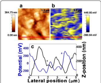
Figure 2 shows topography, surface potential, and the line profiles of the CZTSSe thin film. Grains of the CZTSSe films are shown in Figure 2a. The grains seem to possess small particulates. In Figure 2b, yellow region represents positive potential value and blue region indi-cates negative potential value. The one-dimensional line profiles in Figure 2c project the blue line of Figure 2a,b. In Figure 2c, the CZTSSe thin film reveals high positive
surface potential near GBs. CIGS thin films form po-sitively charged GBs which is related to negative band bending. The negative energy bending near GBs improves carrier separation and suppresses recombination of elec-tron–hole pairs at GBs [14,15] because holes tend to be kept away from the GB region. However, the minority-carrier electrons are moving into the GBs, which might be a traoff for carrier migration to the electrodes. It is de-sirable to study carrier transport in the intragrains (IGs) as well as the GBs. Surface potential distribution in the CZTSSe thin film shows similar behaviors to the CIGS thin films. The potential near GBs in the CZTSSe thin film indicates about 300 mV and negative potential about−100 to −200 mV at IGs, which is linked to negative band bending on GBs of the CZTSSe thin film. This is consistent with the fact that some of the minority carriers (electron) transferred to and collected at GBs in the CZTSe thin film [25]. Thus, electron–hole carriers separ-ate effectively on GBs of CZTSSe thin film not acting as recombination center, which is a similar phenomenon oc-curring in CIGS. In order to clarify the relationship be-tween topography and surface potential, we introduce a topographic parameterΦ = d2H/dX2. H is the height and X is the lateral direction. So the second derivative of H with respect to X means the concave or the convex shapes of the surface topography. SinceΦ is an indicative of the surface alterations of the films, we can expect the positive value as GBs and the negative as IGs. From this parameter, we are able to ascertain roughly the region of GBs on the surface. Some groups claim that additional information like electron beam backscattered diffraction (EBSD) is re-quired to confirm the granular nature of the local regions [26]. However, our approach is also widely acceptable for inspection of the surface topography and potential. The
Table 1 Device performances and composition of CZTSSe thin-film solar cell
Sample Voc(mV) Jsc(mA/cm2) F.F. (%) Eff. (%) Cu/ Zn + Sn
Zn/Sn
CZTSSe 349.00 30.61 46.13 4.93 0.94 1.65
Figure 2 Topography (a), corresponding potential images (b), and one-dimensional line profile (c) of the CZTSSe thin film.
experimental results on the relationship between potential and surface are verified, but the implications of the rela-tionship will be further investigated in particular for the regard of conversion efficiency.
Conductive atomic force microscopy
Figure 3 shows topography, current map, and the line profiles of the CZTSSe thin film. Local current flows up to larger than 6 nA on GBs in the CZTSSe thin film. In case of CIGS, magnitude of current showed about 2 nA under the sample external voltage of 0.2 V [27]. The CZTSSe thin film exhibits local current flowing mostly near the GBs as displayed in Figure 3c. Local current routes are formed near the GBs of the CZTSSe thin film. The one-dimensional line profile shows the current flows at the edge of the grains. Similar current distribu-tion was observed in the GBs of the CIGS thin films [28,29]. Azulay et al. proposed that higher dark current flow through the GBs because of higher hole mobility on the GBs and then inversion of the dominant carrier type at the GBs [29]. Therefore, electrons can become domin-ant carriers in GBs and drift along GBs of the CIGS thin films [27,29]. From C-AFM measurement, we can sug-gest that collected minority carriers form local current route through the near GBs in the case of the CZTSSe thin film, indicating that it is possible that carrier type inversion can also happen in the CZTSSe thin films.
From the measurement results of KPFM and C-AFM, we found positive potential on the most of GBs and demonstrated downward band bending in the CZTSSe thin film. On the other hand, the negative potential on the GBs is linked to the upward band bending. A model
of surface potential and carrier transport is described in Figure 4. The positively charged GBs play a role to be a conduction path and collect minority carriers. However, the defects in the GBs are not well known yet. So, the carriers can be trapped in the defects near the GBs [30], which may be drawbacks for high efficiency of the CZTSSe solar cells. The model of band diagram depends on charged GBs can be affected by film properties such as composition and conversion efficiency [20]. It is indispen-sible to understand the defect chemistry and transport near GBs of the CZTSSe. If all the understandings are well established and proper processing methods are developed, polycrystalline kesterite thin films are beneficial to device performance for solar cells.
Conclusions
We measured surface potential and current transport of the CZTSSe thin film with Kelvin probe force micros-copy and conductive atomic force microsmicros-copy, respect-ively. For these studies can demonstrate the essential of combining local electrical characterization techniques to investigate the local current and potential properties of kesterite materials. The surface potential near GBs shows negative band bending behaviors with about 300 meV of energy shift. In the current map, the dominant current flow path is observed through GBs, which is governed by minority carriers. Most of the electrical properties of the CZTSSe are very similar to the CIGS, but we will study more the details to explain the physical and chemical properties in the interface of the CZTSSe thin films for high conversion efficiency.
Figure 3 Topography (a), corresponding current-map images (b), and one-dimensional line profile (c) of the CZTSSe thin film.
Figure 4 A proposed band bending near the GBs of the CZTSSe thin films. The band diagram also accounts for the minority carrier transport near the GBs.
Abbreviations
C-AFM:Conductive atomic force microscopy; CIGS: Cu(In,Ga)Se2; CZTSSe: Cu2
(Zn,Sn)(S,Se)4; EBSD: Electron beam backscattered diffraction; Eff.:
Photo-conversion efficiency; F.F.: Fill factor; GBs: Grain boundaries; IGs: Intragrains; Jsc: Short circuit current; KPFM: Kelvin probe force microscopy; Voc: Open
circuit voltage.
Competing interests
The authors declare that they have no competing interests.
Authors’ contributions
GYK, JRK, and WJ measured the electrical properties of the CZTSSe samples with scanning probe microscopy. DHS, DHK, and JKK made the CZTSSe samples by sputtering and subsequent selenization. All authors read and approved the final manuscript.
Acknowledgements
This work was supported by the New & Renewable Energy of the Korea Institute of Energy Technology Evaluation and Planning (KETEP) grant funded by the Korea government Ministry of Trade, Industry, and Energy (No. 20123010010130).
Author details
1Department of Physics, Ewha Womans University, Seoul 120-750, Korea. 2Advanced Convergence Research Center, Daegu Gyeongbuk Institute of Science and Technology (DGIST), Daegu 711-873, Korea.
Received: 4 October 2013 Accepted: 9 December 2013 Published: 8 January 2014
References
1. Chen S, Gong XG, Walsh A, Wei S-H: Electronic structure and stability of quaternary chalcogenide semiconductors derived from cation cross-substitution of II-VI and I-III-VI2compounds. Phys Rev B 2009, 79:165211.
2. Todorov TK, Tang J, Bag S, Gunawan O, Gokmen T, Zhu Y, Mitzi DB: Beyond 11% efficiency: characteristics of state-of-the-art Cu2ZnSn(S, Se)4solar
cells. Adv Energy Mater 2013, 3:34–38.
3. W-C H, Repins I, Beall C, DeHart C, To B, Yang W, Yang Y, Noufi R: Growth mechanisms of co-evaporated kesterite: a comparison of Cu-rich and Zn-rich composition paths. Prog Photovolt: Res Appl 2014, 22:35–43. 4. Repins I, Beall C, Vora N, DeHart C, Kuciauskas D, Dippo P, To B, Mann J,
W-C H, Goodrich A, Noufi R: Co-evaporated Cu2ZnSnSe4films and devices.
Sol Energy Mater Sol Cells 2012, 101:154–159.
5. Hiroi H, Sakai N, Kato T, Sugimoto H: High voltage Cu2ZnSnS4submodules
by hybrid buffer layer. In Proceedings of the IEEE Photovoltaic Specialists Conference 39th: 16–21 June 2013. Tampa, FL.
6. Katagiri H, Jimbo K, Maw WS, Oishi K, Yamazaki M, Araki H, Takeuchi A: Development of CZTS-based thin film solar cells. Thin Solid Films 2009, 517:2455–2460.
7. Shin SW, Pawar SM, Park CY, Yun JH, Moon J-H, Kim JH, Lee JY: Studies on Cu2ZnSnS4(CZTS) absorber layer using different stacking orders in
precursor thin films. Sol Energy Mater Sol Cells 2011, 95:3202–3206. 8. Zoppi G, Forbes I, Miles RW, Dale PJ, Scragg JJ, Peter LM: Cu2ZnSnSe4thin
film solar cells produced by selenization of magnetron sputtered precursors. Prog Photovolt: Res Appl 2009, 17:315–319.
9. Scragg JJ, Ericson T, Fontané X, Izqierdo-Roca V, Pérez-Rodríguez A, Kubart T, Edoff M, Platze-Björkman C: Rapid annealing of reactively sputtered precursors for Cu2ZnSnS4solar cells. Prog Photovolt: Res Appl. 2014, 22:10–17.
10. Momose N, Htay MT, Yudasaka T, Igarashi S, Seki T, Iwano S, Hashimoto Y, Ito K: Cu2ZnSnS4thin film solar cells utilizing sulfurization of metallic
precursor prepared by simultaneous sputtering of metal targets. Jpn J Appl Phys 2011, 50:01BG09.
11. Araki H, Kubo Y, Mikaduki A, Jimbo K, Maw WS, Katagiri H, Yamazaki M, Oishi K, Takeuchi A: Preparation of Cu2ZnSnS4thin films by sulfurizing
electroplated precursors. Sol Energy Mater Sol Cells 2009, 93:996–999. 12. Jimbo K, Kimura R, Kamimura T, Yamada S, Maw WS, Araki H, Oishi K,
Katagiri H: Cu2ZnSnS4-type thin film solar cells using abundant materials.
Thin Solid Films 2007, 515:5997–5999.
13. Jackson P, Hariskos D, Lotter E, Paetel S, Wuerz R, Menner R, Wischmann W, Powalla M: New world record efficiency for Cu(In, Ga)Se2thin-film solar
cells beyond 20%. Prog Photovolt: Res Appl 2011, 19:894–897.
14. Jiang C-S, Noufi R, AbuShama JA, Ramanathan K, Moutinho HR, Pankow J, Al-Jassim MM: Local built-in potential on grain boundary of Cu(In, Ga)Se2
thin film. Appl Phys Lett 2004, 84:3477–3479.
15. Jiang C-S, Noufi R, Ramanathan K, AbuShama JA, Moutinho HR, Al-Jassim MM: Does the local built-in potential on grain boundaries of Cu(In, Ga) Se2thin films benefit photovoltaic performance of the device? Appl Phys
Lett 2004, 85:2625–2627.
16. Yan Y, Jiang C-S, S–H W, Moutinho HR, Al-Jassim MM: Electrically benign behavior of grain boundaries in polycrystalline CuInSe2Films. Phys Rev
Lett 2007, 99:235504.
17. Persson C, Zunger A: Compositionally induced valence-band offset at the grain boundary of polycrystalline chalcopyrites creates a hole barrier. Appl Phys Lett 2005, 87:211904.
18. Abou-Ras D, Schaffer B, Schaffer M, Schmidt SS, Caballero R, Unold T: Direct insight into grain boundary reconstruction in polycrystalline Cu(In, Ga) Se2with atomic resolution. Phys Rev Lett 2012, 108:075502.
19. Takihara M, Minemoto T, Wakisaka Y, Takahashi T: An investigation of band profile around the grain boundary of Cu(In,Ga)Se2solar cell material by
scanning probe microscopy. Prog Photovolt: Res Appl 2013, 21:595–599. 20. Jeong AR, Jo W, Jung S, Gwak J, Yun JH: Enhanced exciton separation
through negative energy band bending at grain boundaries of Cu2ZnSnSe4thin-films. Appl Phys Lett 2011, 99:082103.
21. Mönig H, Smith Y, Caballero R, Kaufmann CA, Lauermann I, Lux-Steiner MC, Sadewasser S: Direct evidence for a reduced density of deep level defects at grain boundaries of Cu(In, Ga)Se2thin films. Phys Rev Lett 2010,
105:116802.
22. Azulay D, Balberg I, Millio O: Microscopic evidence for the modification of the electronic structure at grain boundaries of Cu(In1-x, Gax)Se2films.
Phys Rev Lett 2012, 108:076603.
23. Melitz W, Shen J, Kummel AC, Lee S: Kelvin probe force microscopy and its application. Surf Sci Rep 2011, 66:1–27.
24. Guo Q, Ford GM, Yang W-C, Walker BC, Stach EA, Hillhouse HW, Agrawal R: Fabrication of 7.2% efficient CZTSSe solar cells using CZTS nanocrystals. J AM CHEM SOC 2010, 132:17384–17386.
25. Li JB, Chawla V, Clemens BM: Investigating the role of grain boundaries in CZTS and CZTSSe thin film solar cells with scanning probe microscopy. Adv Mater 2012, 24:720–723.
26. Sadewasser S, Abou-Ras D, Azulay D, Baier R, Balberg I, Cahen D, Cohen S, Gartsman K, Ganesan K, Kavalakkatt J, Li W, Millo O, Rissom T, Rosenwaks Y, Schock H-W, Schwarzman A, Unold T: Nanometer-scale electronic and microstructural properties of grain boundaries in Cu(In, Ga)Se2. Thin Solid
Films 2011, 519:7341–7346.
27. Shin RH, Jo W, Kim D-W, Yun JH, Ahn S: Local current–voltage behaviors of preferentially and randomly textured Cu(In, Ga)Se2thin films investigated
by conductive atomic force microscopy. Appl Phys A 2011, 104:1189–1194. 28. Shin RH, Jeong AR, Jo W: Investigation of local electronic transport and surface potential distribution of Cu(In, Ga)Se2thin-films. Curr Appl Phys
2012, 12:1313–1318.
29. Azulay D, Millo O, Balberg I, Schock HW, Visoly-Fisher I, Cahen D: Current routes in polycrystalline CuInSe2and Cu(In, Ga)Se2films. Sol Energy Mater
Sol Cells 2007, 91:85–90.
30. Li J, Mitzi DB, Shenoy VB: Structure and electronic properties of grain boundaries in earth-abundant photovoltaic absorber Cu2ZnSnSe4.
ACS Nano 2011, 5:8613–8619.
doi:10.1186/1556-276X-9-10
Cite this article as: Kim et al.: Nanoscale observation of surface potential and carrier transport in Cu2ZnSn(S,Se)4thin films grown by