P2-1 / S. E. Chung
• IMID 2009 DIGEST
Abstract
We demonstrate conformal phosphor coating and patterning methods on light emitting diodes (LEDs) using image processing based optofluidic maskless lithography (IP-OFML) system in microfluidic channels. IP-OFML allows a real-time detection and dynamic mask generation for packaging of randomly dispersed microchips. Our system detects each chip by considering rotation of the chip through image processing regardless of their arrangement error. Therefore, it precisely packages the chip making conformal polymer layer.
1. Introduction
Commercial phosphor coating technology of LED suffers from high cost of production and non-uniformity of coating layers [1]. Since uniform light emission from the LED depends on the uniformity of the phosphor layer surrounding an LED chip, conformal phosphor coating technique with low cost of production and high accuracy is required. To overcome the limitations of current conformal coating technologies, various phosphor coating technologies have been tried by several groups [2-3]. However, these technologies still have complex fabrication processes and they are time-consuming processes. Recently presented our OFML technique, a dynamic in situ photopolymerization method using MEMS spatial light modulator [4], can be optimized to conformal chip packaging process combined with image process aided by computer-vision [5]. Here, we developed image processing based OFML system to package and pattern conformal polymer layers on silicon microchips and light emitting devices. Multi-layer coating and selective Multi-layer coating are demonstrated using silicon microchips, and top surface patterning for efficient wire-bonding from N-/P-type contact to lead frame reducing production cost.
2. Experimental
Fig. 1 schematically describes an overall IP-OFML system. When CCD takes an image of externally introduced microchips mixed with polymer resin within a fluidic channel, the image is transferred to the computer for DMD mask generation via image processing. Corresponding DMD mask for packaging is loaded onto DMD, and patterned UV light is exposed to the originally dispersed chips. This individual chip detection allows precise packaging of the chips considering their location and rotation.
Figure 1. (a) Schematic diagram of image processing based optofluidic maskless lithography method (b)-(g) Image processing for polymer coatin
3. Results and discussion
For the case of randomly placed chips on the substrate, the lithography process using fixed photomask is inefficient making uniformity errors. Since our system detects each chip by considering one’s rotation via image processing regardless of their arrangement error, it precisely packages the chip making conformal polymer layer. Conformal three layers are packaged by sequentially introducing and packaging each different material one by one for each layer (Fig. 2(a)). Furthermore, the fabrication of light guiding lens structure applicable to edge-emitting LED is also presented for advanced light expansion of
Optofluidic packaging and patterning technologies for
light emitting devices
Su Eun Chung
1,2, Jisung Jang
1,2a, Seung Ah Lee
1,2, Hosuk Lee
1, and
Sunghoon Kwon
1,21
School of Electrical Engineering and Computer Science, Seoul National University, Seoul 151-744, Korea
TEL:82-2-880-1736, e-mail: skwon@snu.ac.kr 2
Inter-university Semiconductor Research Center, Seoul National University, Seoul 151-744, Korea
P2-1 / S. E. Chung
IMID 2009 DIGEST • focusing to the panel (Fig. 2(b)).
Figure 2. (a) Multilayer heterogeneous polymer packaging (b) Lens structure fabrication for light guiding (c) Top surface patterning for external contacts
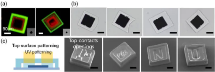
In addition, we packaged top surfaces of both silicon chips (Fig. 2(c)) and LEDs (Fig. 3(a)) with various patterns by just substituting desired image on DMD during IP-OFML. Each LED has contacts for the external power connection, and these contacts should not be coated with phosphors. Commercial technology executes wire-bonding for the contacts first, and then packaging of the chip. So, if defects are observed on the chip after coating, the whole expenditure is irreversible. Since IP-OFML uses one-time exposure by patterning opened top contacts before wire-bonding, unnecessary process can be reduced. With our top surface patterning method, we demonstrate phosphor coating, mixed in polymer resin, on blue LED dies for white light illumination (Fig. 3(b)).
Figure 3. (a) Polymer top surface patterning on blue LED die (blue luminescence) (b) Yellow phosphor top surface patterning on blue LED die (white light illumination)
4. Summary
Conformal phosphor coating on LED is required for uniform illumination at wide-range of viewing angle. We showed conformal multilayer polymer coating and lens fabrication on silicon chips, and yellow phosphor coating on blue LED dies. Due to the continuity and the high-yield of the process, we expect that this technique can find numerous applications in the advanced LED packaging technology.
5. References
1. J. Yun, S. Kim, Y. Sung, Colloids and Surfaces A,
251, 203 (2004).
2. K. H. Lee, S. W. R. Lee, Electronics Packaging Technology Conference, 379 (2006)
3. J. Yum, S. Seo, S. Lee, Y. Sung, Journal of the Electrochemical Society, 150, H47 (2003) 4. S. E. Chung, W. Park, H. Park, K. Yu, N. Park, S.
Kwon, Applied Physics Letters, 91, 041106 (2007). 5. S. E. Chung, S. A. Lee, J. Kim, S. Kwon, Lab on a
Chip, DOI: 10.1039/ B903760H (2009)
6. Acknowledgements
This work was partly supported by System IC 2010 project and Strategic Technology Development Project of the Ministry of Knowledge Economy and IT R&D program of MKE/IITA [0414-20090013].