https://doi.org/10.6113/JPE.2019.19.6.1429 ISSN(Print): 1598-2092 / ISSN(Online): 2093-4718
JPE 19-6-8
Digital Implementation of Optimal Phase Calculation
for Buck-Boost LLC Converters
Qinsong Qian
*, Bowen Ren
*, Qi Liu
*, Chengwang Zhan
*, and Weifeng Sun
††,*Department of Electronic Science and Engineering, Southeast University, Nanjing, China
Abstract
Buck-Boost LLC (BBLLC) converters based on a PWM + phase control strategy are good candidates for high efficiency, high power density and wide input range applications. Nevertheless, they suffer from large computational complexity when it comes to calculating the optimal phase for ZVS of all the switches. In this paper, a method is proposed for a microcontroller unit (MCU) to calculate the optimal phase quickly and accurately. Firstly, a 2-D lookup table of the phase is established with an index of the input voltage and output current. Then, a bilinear interpolation method is applied to improve the accuracy. Meanwhile, simplification of the phase equation is presented to reduce the computational complexity. When compared with conventional curve-fitting and LUT methods, the proposed method makes the best tradeoff among the accuracy of the optimal phase, the computation time and the memory consumption of the MCU. Finally, A 350V-420V input, 24V/30A output experimental prototype is built to verify the proposed method. The efficiency can be improved by 1% when compared with the LUT method, and the computation time can be reduced by 13.5% when compared with the curve-fitting method.
Key words: Buck-boost LLC, LUT, MCU, Phase, Simplified bilinear interpolation
I. I
NTRODUCTIONIn recent years, the efficiency of power supplies has become a popular issue due to the great increase in electricity consumption in various fields. The demand for creating a high efficiency and high power density DC/DC converter with a wide input voltage range is expected to noticeably increase. The LLC resonant converter is widely adopted due to its small number of elements and its ability to realize a wide zero-voltage-switching (ZVS) range [1]-[3]. However, LLC resonant converters cannot maintain high efficiency over a wide input voltage range. A substantial volume of research has been carried out [4]-[7] for improving the range of input voltage.
Two-stage architectures have been verified to be advantageous for achieving a wide input voltage range and high efficiency [5]. However, these two-stage converters need complex control, and are mostly implemented in FPGA and
complex analog controlled circuits. The area and price of FPGAs with analog circuits restrict two-stage converters to applications for commercial use.
Since digital controllers are gradually taking the place of analog controllers in the switching power supply, MCUs are preferred due to their low cost and small area [6], [7]. For two-stage converters, it is meaningful to create a suitable digital control method to be implemented in MCUs. However, the memory and instruction cycle of MCUs are limited. Thus, digital control algorithms cannot be complicated or use excessive data.
In this paper, the digital control of a buck-boost LLC (BBLLC) converter is discussed. The BBLLC converter cascades a buck-boost converter with an LLC resonant converter [8], [9], which can be implemented by the fixed frequency control strategy. In this converter, the PWM + phase shift control is adopted, which can regulate the duty ratio of buck-boost converter to shrink the input voltage range of the LLC resonant converter. Therefore, the BBLLC converter can work over wide voltage range and achieve a high conversion efficiency. Additionally, in order to realize ZVS of the switches and reduce conduction loss, the optimal phase needs to be calculated.
There are three conventional digital control methods for © 2019 KIPE
Manuscript receivedDec. 15, 2018; accepted Aug 4, 2019 Recommended for publication by Associate EditorWu Chen.
†Corresponding Author: swffrog@seu.edu.cn
Tel: +86-025-83795811, Southeast University
*Department of Electronic Science and Engineering, Southeast University,
calculating phase. These methods include constant phase, establishing a theoretical model [10], [11], look-up table (LUT) [8], [9], [12], etc. The phase is relative to the duty ratio, deadtime, input and so on. Thus, building a model for the optimal phase is so complicated that an MCU cannot achieve it in a short time. In addition, a BBLLC converter using a constant phase cannot achieve a high efficiency under different situations. Hence, measuring the optimal phase in advance is a suitable choice. However, using the curve-fitting method for calculating the phase leads to a complicated formula [13], which includes high-order terms of the input voltage and output current. This method may increase the computation time and the period of regulation for the phase, which affects the performance of the dynamic response. Additionally, for the purpose of creating a table of the phase to ensure high efficiency under different conditions, more data needs to be measured. In addition, it is difficult for a MCU to store this data. Therefore, a method named simplified bilinear interpolation LUT is proposed to combine simplified bilinear interpolation with a LUT to solve the problems of conventional methods.
The simplified bilinear interpolation LUT (SBILUT) method can reduce computation time and save memory, which is appropriate for low-cost MCUs. This method measures the optimal phase under different working conditions in advance. This data is then used to establish a 2-D table based on the input voltage and output current. In addition, the scope of the working conditions is divided into different working regions. Meanwhile, the slope of the optimal phase between adjacent working regions is also recorded. In actual work, if the optimal phase under the current working state is recorded in the table, it can be immediately used to control the converter. When the optimal phase cannot be found, four adjacent phases and a bilinear interpolation algorithm are used to calculate the optimal phase. Additionally, the expression of the optimal phase can be simplified based on numerical analysis. The computation time of the expression is significantly reduced through an approach to cut down the count for using the slope variable. In addition, the period of regulation for the phase is decreased, leading to a low system cost. A detailed analysis and the control strategy are given in Section 4.
The major contribution of this paper is to propose an improved method for calculating the optimal phase in a BBLLC converter with a low-cost MCU. This paper is organized as follows. A topology description of the buck- boost LLC converter and an ideal model of the phase are discussed in Section II. Section III shows conventional methods for calculating the optimal phase. In Section IV, the operating principle and control strategies of the proposed method are described in detail. In order to verify the proposed method, experimental results obtained from a prototype converter system are demonstrated in Section V. Finally, some conclusions and suggestions for future work are presented in Section VI.
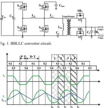
Fig. 1. BBLLC converter circuit.
Fig. 2. Key operation waveforms of a buck-boost LLC converter.
II. T
OPOLOGYD
ESCRIPTION OF THEB
UCK-
BOOSTLLC
C
ONVERTERA. Working Waveforms and Parameter Definition
As shown in Fig. 1, a buck-boost converter consists of the switches S1, S2, S3, S4 and the inductor Lb. Meanwhile, the
LLC resonant converter consists of the switches S3, S4, SR1,
SR2, the inductors Lr, Lm, and the capacitor Cr. The buck-
boost LLC converter cascades a buck-boost converter with an LLC resonant converter, which is appropriate for a wide input voltage range. In addition, improving the design of the resonant parameters can keep the LLC resonant converter working at around resonance point to ensure a high efficiency [1], [2].
Fig. 2 presents key operation waveforms of a buck-boost LLC converter. S1 and S2 are complementary, and S3 and S4
are complementary, ignoring the deadtime. Additionally, D is defined as the duty ratio of S1 in one cycle, and P is the phase
shift between S4 and S1. In addition, the duty ratio of S3 and
S4 keeps 0.5 in one cycle. Furthermore, assuming the phase is
always greater than zero, there are only four stages in the buck-boost converter. The corresponding equivalent circuits in one period are shown in Fig. 3.
Stage 1 [t0-t1]: Before t0, the current of the inductor Ib
charges the stray capacitance of S1 (Coss1) while discharging
the stray capacitance of S2 (Coss2). Owing to Ib, the electric
potential of ‘a’-Va rises to the input voltage Vin, which is
helpful for achieving ZVS of S1. At the beginning of this
cycle (t=t0), S1 turns on and Vin provides energy, making Ib
have a positive increase. In this stage, the resonance current Ir
is always less than the exciting current ILm. Thus, in the
secondary side, SR2 supplies the output voltage.
Vout+ Vout-S1 S2 S3 S4 Lb Lr Transformer SR1 SR2 RL Cr Cin Lm Cbus CL Vin D ·T P ·T S3 S4 S3 S4 S3 S4 S3 S1 S2 S1 S2 S1 S1 t0 t1 t2 t3 t4 1 2 3 4 S2 Ir ILm Ib
Fig. 3. Equivalent circuits for different time intervals in one switching cycle.
Stage 2 [t1-t2]: Before t1, with the combined action of Ib and
Ir, S3 can easily realize ZVS, which can always be regarded as
a ZVS switch. When t=t1, S3 turns on, and Vin with the
voltage of Cbus-Vbus provides energy. If Vin is greater than Vbus,
Ib increases. Otherwise, Ib falls. When Vin is equal to Vbus, Ib
remains unchanged as in Fig. 2. Theoretically speaking, according to the operating principle of the buck-boost converter [14], [15]:
(1)
(2)
Since the gain of the LLC resonant converter G is constant in this converter, adjusting the duty ratio D can stabilize Vbus,
which can also regulate the output voltage Vo. When the
converter begins to work, Cbus accumulates energy and ensure
that Vbus gradually rises until the steady state. The steady-
state value of Vbus depends on many factors such as the
output voltage, the gain of the transformer, the input range and so on. In this paper, since the gain of the LLC resonant converter is a fixed value under the steady state, Vbus does not
need to be adjusted. In fact, the regulation and stabilization of Vo are equivalent to adjusting Vbus.
Stage 3 [t2-t3]: Before t2, Ib charges Coss2 while discharging
Coss1. The electric potential of ‘b’- Vb falls to zero, which is
helpful for achieving ZVS of S2. At the beginning of this
stage, S2 turns on and Vbus provides energy, which makes Ib
have a negative decrease. During stage 2 and stage 3, Ir is
always greater than ILm. Thus, in the secondary side, SR1
supplies the output voltage.
Stage 4 [t3-t4]: Compared with S3, Ib and Ir work together to
supply energy for the ZVS of S4. In this interval, S2 and S4
work so that Ib stays stable until the end of the cycle. In
addition, Ir is always less than ILm. Thus, in the secondary
side, SR2 turns on while SR1 turns off.
Based on the above analysis, all of the switches can realize ZVS to improve efficiency. However, whether the power switches realize ZVS depends on the value of the phase. The importance and model of the phase are discussed in the next part.
Fig. 4. Different phase influences Ib under the same working
conditions.
Fig. 5. Different Io influences Ib. (a) When using a constant phase.
(b) When using the optimal phase.
B. Influence of Phase on Loss
As mentioned above, it is vital that Ib provides enough
energy to realize ZVS of S1 and S2. When the duty ratio D is
stable, Ib is only relative to the phase between S4 and S1,
while ignoring the deadtime. The black line in Fig. 4 represents the optimal Ib, which is just enough for fully
charging Coss1 or Coss2. If the phase decreases, like the blue
line in Fig.4, both the amplitude and the DC offset of Ib
increase. Although this can realize ZVS of S1 and S2, it leads
to high conduction loss in all of the switches. Otherwise, both the amplitude and the DC offset of Ib decrease. It is possible
to lead to hard-switching of S1 and S2, which reduces the
efficiency of the BBLLC converter.
Additionally, if the converter uses a constant phase under different working conditions, it reduces efficiency. Fig. 5 (a) shows waveforms of Ib under different loads. The blue line,
black line and red line represent a 30% load, 50% load and 80% load, respectively. If phase is kept unchanged, Ib
changes from the blue line to the red line in Fig. 5 (a) at a heavy load. Although it can realize ZVS of S2, the DC offset
of Ib cannot provide enough energy for S1 to realize ZVS,
which increases the switching loss. When converter uses the optimal phase under different working conditions, as shown in Fig. 5 (b), the amplitude and the DC offset of Ib are close
under different loads. This can just fully charge Coss1 or Coss2,
while reducing the conduction loss and switching loss. Therefore, it is essential for the converter to find a control strategy to calculate the optimal phase accurately under different working conditions.
SR1 S3 S4 S1 S2 Lr Lm Vbus Vin Lb Cr Cbus Cin S3 S4 S1 S2 Lr Lm Vbus Vin Lb Cr Cbus Cin S3 S4 S1 S2 Lr Lm Vbus Vin Lb Cr Cbus Cin S3 S4 S1 S2 Lr Lm Vbus Vin Lb Cr Cin (Stage 1) (Stage 2) (Stage 3) (Stage 4) a b a b a b a b SR2 Cbus SR1 SR2 CL SR1 SR2 CL SR1 SR2 RL RL RL RL CL CL Vin Vin Vin Vin bus 0.5 in D V V o bus V G V
t
I
bS
aS
b-I
0 P·T D· T large small t Ib -I0 P· T D·T (a) Ib -I0 P· T D·T (b) tFig. 6. Control structure for the proposed method.
C. Analysis and Ideal Model of the Phase
The operating principle of the BBLLC was discussed in the previous part. It can be assumed that the minimum value of Ib is -Imin. Hence, in a period, the expression of Ib can be
achieved as:
(3)
In Fig. 4, Sa-Sb is the area surrounded by Ib and the zero
axis, which represents electric quantity transported from Vin
to the converter. Meanwhile, the time of each stage is discussed in part A. Thus, the input power can be expressed as:
(4)
(5) From formula (5), it can be seen that P has no linear dependence relation with Vin and Io. In addition, formula (5)
has more than 10 operations and root square operations. This results in a long computation time, which affects the dynamic performance of the BBLLC converter. In consideration of the complexity of equation (5), the most appropriate phase is difficult for a MCU to solve.
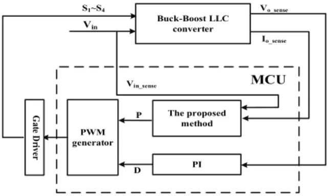
Hence, a new method to simplify the operations to calculate the optimal phase under different working conditions is important. Fig. 6 shows the control structure of the proposed method. This method has been implemented on a STM32F334 from ST. The MCU samples the output voltage Vo, input voltage Vin and output current Io. The optimal phase
can be calculated by these sampled values with the proposed method, which reduces both the computational complexity and memory consumption.
Fig. 7. Optimal phase under different working conditions.
III. V
ARIETY OFD
IFFERENTA
PPROACHES FORC
ALCULATING THEO
PTIMALP
HASEFrom equation (5), the expression for calculating the optimal phase consists of four addition or minus operations, nine multiplication or division operations and two root square operations. It is so complicated that MCU cannot find the result of expression (5) in a short time, especially for high- switching converters like the BBLLC converter.
Thus, in order to simply obtain the optimal phase, a large number of methods has been proposed. Since it is hard to directly calculate the optimal phase, the optimal phase can be measured in advance in an open loop test. In the open loop test, a phase is chosen according to equation (5) and the actual correction under different conditions. A phase can be recorded as the optimal phase when the converter works at top efficiency. When the open loop test consists of all working conditions, the optimal phase can be obtained and recorded in a 2-D Table. Fig. 7 shows optimal phases under different working conditions.
In actual work, the recorded phase needs to be written in an MCU to control a BBLLC converter to work at peak efficiency. When writing these data in the MCU, the curve- fitting method and a look-up table (LUT) are the most common methods for converters.
Curve-fitting: As shown in Fig. 7 and equation (5),
although Vin and Io can be used to accurately fit the optimal
phase, this leads to higher order terms of Vin and Io. For
example, if 350<Vin<370, the expression of the optimal phase
is as follows:
(6) Although the determination coefficient of equation (6) is 0.9954, working out equation (6) is difficult for the MCU. In equation (6), it consists of five addition or minus operations and eight multiplication or division operations. It is practical for the MCU to solve the optimal phase. However, it may take MCU long time for the calculations.
Vo_sense Io_sense S1~S4 PI The proposed method PWM generator P MCU Buck-Boost LLC converter D Ga te Dr iv er Vin Vin_sense min min b min min [0, ] [ ,0.5 ] i ( ) 0.5 [0.5 ,( ) ] 0.5 [( ) , ] in b in bus b b in bus b b I t PT V I t PT t PT T L t I V t PT V t T t T D P T L L V V I DT t T t D P T T L L 2 2 2 min 0.5 2 2 o o o in in bus in in in a b in b b P V I P V V D P T V D T P V S S V I DT L L 2
2 2 in in min b o b 0.5 in bus D V D V I L T P L P D V V T 15.0 17.5 20.0 22.5 25.0 27.5 30.0 0.32 0.36 0.40 Vin=350V Vin=385V Vin=420V ph as e Io/A 2 2 1+k2 in 3 4 5 6 Pk V k Io k Vin k Vin Io k Io LUT: Additionally, a LUT can decrease the computation
time by reducing the number of operations. However, in order to make the converter work at a high efficiency under different conditions, at least a 29*16 matrix needs to be recorded in the MCU. Since a number with the float type occupies at least 4 bytes in the MCU, a 29*16 matrix requires about 2 Kbytes. In this converter, a STM32F334 is used to store this data. Only 12 Kbytes of SRAM can be provided, which cannot store a large amount of data for the LUT due to other control variables in the MCU.
Thus, conventional methods are not suitable for calculating the optimal phase with a MCU. The curve-fitting method can obtain the proper phase accurately except. However, it wastes time, resulting in a high system cost. A LUT can save calculation time, but consumes too much memory. Therefore, a method to calculate the proper phase with a MCU needs to be proposed.
IV. P
ROPOSEDO
PERATINGP
RINCIPLE ANDC
ONTROLS
TRATEGIESIn this paper, a simplified bilinear interpolation LUT (SBILUT) is proposed to calculate the optimal phase under different working conditions. This method combines a LUT with bilinear interpolation, which makes a tradeoff between the memory of the MCU and the calculation of the optimal phase.
A. Principle of Bilinear Interpolation
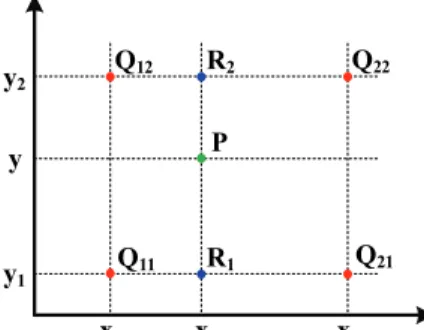
The earliest application of the bilinear interpolation algorithm was involved in image processing [16], [17], where it was used to improve the accuracy of data calculation and to reduce resource consumption. Fig. 8 shows four pixels Q11,
Q12, Q21 and Q22 in one image. If the value of P needs to be
obtained, bilinear interpolation can be used with the four adjacent pixels Q11, Q12, Q21 and Q22.
(7)
(8)
Firstly, linear interpolations are made in the x-direction to obtain the values of R1 and R2. Here kx1 is the slope between
Q11 and Q21, while kx2 is the slope between Q12 and Q22.
Then, linear interpolations are made in the y-direction to obtain the value of f(P). here ky1 is the slope between Q11 and
Q12, while ky2 is the slope between Q21 and Q22. The slope of
P can be calculated by ky1 and ky2.
(9)
Fig. 8. General view of bilinear interpolation.
(10)
Therefore, the value of f (P) is as follows:
(11)
Equation (11) also has complicated operations, which take the MCU a lot of time to obtain a result. Thus, in the converter, equation (11) is simplified to be used in the proposed method to calculate the proper phase. A mathematical analysis and concrete steps for simplification in the SBILUT are discussed in the next part.
B. Important Assumption of the SBILUT for Calculating the Optimal Phase
The SBILUT is similar to a LUT, which needs to measure and record the optimal phase under different working conditions. However, in equation (11), it consists of seven addition or minus operations and five multiplication or division operations. Additionally, it uses the values of kx1, ky1
and ky2, which need to be simplified through mathematical
analysis and assumption.
The important condition for the correctness of this assumption is that the efficiency of the converter is similar under two adjacent Vin. The optimal phase is measured under
different Vin and Io. If Io or the load changes, with close
efficiency, the increment of the power transferred from the input to the output is basically the same. Since the duty has no change under two adjacent Vin, the changes of the optimal
phase are basically the same when the output current changes. The mathematical derivations are listed. If Io changes,
through equation (4), the expressions of the input power are:
(12)
12
1 11 1 2 12 1 x-x ( ) x-x x x f R f Q k f R f Q k
1 2 2 1 1 1 2 1 2 2 1 2 2 1 ( ) ( ) x x f Q f Q k x x f Q f Q k x x
( 1) y
1
f P f R k y y x1 x2 y1 y2 y x P R2 R1 Q11 Q12 Q22 Q21 1 2 1 1 2 2 1 1 2 1 2 1 12 11 2 1 22 21 2 1 y y y y y y f R f R x x k k k k y y x x f Q f Q k y y f Q f Q k y y
11 1 1
2
1
1
2 1 2 1 1 ( ) ( ) x y y f P f Q k x x x x k x x k y y x x 2 2 2 1 1 10 o o1 1 1 in1 1 min 1 2 2 2 1 1 11 o o2 1 1 in2 1 min 1 0.5 = = 2 2 0.5 = = 2 2 in bus in in b b in bus in in b b V V D P T V I P V D T V I D T L L V V D P T V I P V D T V I D T L L ΔP1 can be obtained by subtracting the above equations: (13) Since the values of Vo, Vbus, T and Lb are always constant
and ΔP12 is a second order small quantity, (13) can be
simplified to operation (14):
(14) (15) Where C is a constant value, and Vin1(0.5-P10) T represents
the increment of Ib·Lb when the switches S1 and S4 turn on.
From equation (14), the variation of phase can be expressed in operation (16) under two adjacent input voltages.
If the efficiency and the original value of the phase are close under Vin1 and Vin2, it can be seen that the variations of
phase are similar. Therefore, according to (16), it is believed that the values of ΔP are almost the same when the output current changes under two adjacent input voltages.
(16)
Based on this assumption, equation (11) can reduce the count of operations with the use of ky1 to replace ky2,as
shownin equation (17). Detailed measurements are illustrated in the next part.
(17)
C. Implementation of Digital Control for the SBILUT
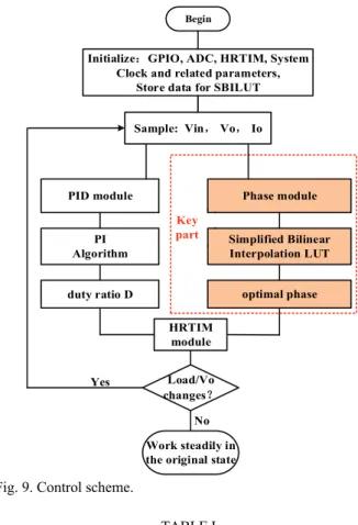
Fig. 9 shows the process of the control strategy. The actual work is based on the optimal phase, which is stored in the MCU. Firstly, initialize each module and store the optimal phase as a two-dimensional array in the MCU. Then, sample the output voltage Vo, the input voltage Vin and the output
current Io all the time. Through the conventional PI algorithm,
duty ratio D can be calculated to keep the output voltage stable. Meanwhile, in order to ensure ZVS in all of the switches and to reduce the conduction loss, the optimal phase needs to be chosen. The SBILUT can calculate the optimal phase under all working conditions. Finally, if the load or Vo
of the converter changes, the converter can regulate the duty ratio D and phase by restarting the proposed strategy.
Since it is the key part of the control scheme, the implementation of the SBILUT needs to be illustrated. When the BBLLC converter works under special working conditions in Table I, the optimal phase can be found immediately. In other cases, a simplified bilinear interpolation algorithm and a LUT are combined to calculate the optimal phase. The specific measures are as follows.
Fig. 9. Control scheme.
TABLE I
OPTIMAL PHASES UNDER DIFFERENT WORKING CONDITIONS
350V 360V … … … … 410V 420V 15A f(Q11) f(Q12) … … … … f(Q17) f(Q18) 20A f(Q21) f(Q22) … … … … f(Q27) f(Q28) 25A f(Q31) f(Q32) … … … … f(Q37) f(Q38) 30A f(Q41) f(Q42) … … … … f(Q47) f(Q48) TABLE II
KXIJ BETWEEN DIFFERENT WORKING CONDITIONS
1 2 3 4 5 6 7 8 1 kx11 kx12 ... ... ... ... kx17 kx18
2 kx21 kx22 ... ... ... ... kx27 kx28
3 kx31 kx32 ... ... ... ... kx37 kx38
4 kx41 kx42 ... ... ... ... kx47 kx48
(1) Vin and Io are adopted as indexes to make a 2-D Table
like Table I.
(2) In an open loop test, a phase is chosen according to equation (5) and an actual correction under different conditions. A phase can be recorded as the optimal phase when the converter works at top efficiency.
(3) As shown in Fig. 9, when the control system begins to initialize, these data are stored as a two-dimensional array in an MCU.
(4) Then, calculate and record kxij and kyij according to
formulas (8) and (10) like Table II and Table III as two- dimensional arrays in the MCU.
o o 1 11 10 1 1 = 2 1 2 in bus b V I V V T P P D P L
1 1 10 1 1 1 10 1 2in (0.5 ) 0.5 2 2bus in(0.5 ) C V T D P P P V T V P T P o o = 2 b bus V I C L V
1 1 10 2 2 20 1 = 2 (0.5 ) 1 = 2 (0.5 ) bus in bus in C P V T V P T C P V T V P T
11 x1 ( 1) y1 ( 1) f P f Q k x x k y y BeginInitialize:GPIO, ADC, HRTIM, System Clock and related parameters,
Store data for SBILUT
PID module Phase module
HRTIM module
Work steadily in the original state
Simplified Bilinear Interpolation LUT duty ratio D optimal phase
Sample: Vin, Vo, Io
Load/Vo changes? Yes No PI Algorithm Key part
TABLE III
KYIJ BETWEEN DIFFERENT WORKING CONDITIONS
1 2 3 4 5 6 7 8
1 ky11 ky12 … … … … ky17 ky18
2 ky21 ky22 … … … … ky27 ky28
3 ky31 ky32 … … … … ky37 ky38
4 ky41 ky42 … … … … ky47 ky48
(5) After the initialization, sample the input voltage Vin, the
output current Io and the output voltage Vo.
(6) Inthe phase module, find a working condition Qij, which
is adjacent to Vin and Io. In addition, calculate the location of
Qij (i, j) in Table I, the variation between Qij and the current
working conditions ΔVin and ΔIo.
(7) As mentioned above, ΔP are almost the same when Io has
the same change under two adjacent Vin. Hence, the difference
between kyij and kyij+1 is so small that kyij+1 can be replaced by
kyij to simplify formula (11):
(18)
(8) Read the values of the adjacent optimal phase f(Qij), kxij,
kyij ΔVin and ΔIo. Through these data and formula (18), the
optimal phase can be calculated under different working conditions according to equation (19).
(19) (9) If the load, Vo or Vin of the converter changes, repeat the
calculation processes (5) - (8) to calculate the appropriate phase.
D. Advantages and Performance of the SBILUT
From the steps mentioned above, the SBILUT method only consists of four addition or minus operations and four multiplication or division operations. In Section III, the curve-fitting method is shown to have five addition or minus operations and eight multiplication or division operations. Due to the first degree of the input voltage and output current in SBILUT, it has a simpler expression to decrease computation time than the curve-fitting method. Additionally, in Section III, it has been analyzed that a LUT needs about 2Kbytes, while the SBILUT only occupies 384 bytes. Although the LUT method has the simplest expression with the fewest operations, the SBILUT can improve the accuracy for calculating the optimal phase and save memory.
In Table IV, the advantages and performance orders of different approaches are listed. It can be seen that the common methods are not appropriate for using an MCU to calculate the optimal phase. The computation time for the optimal phase with the ideal model is the longest, which is not suitable for high speed control. It is rarely adopted due to its computational complexity. The curve-fitting method can accurately obtain the optimal phase. However, it consumes time, leading to a high system cost. Using a LUT can save computation time. However, it consumes too much memory and reduces efficiency. Although
TABLE IV
RANKING OF DIFFERENT METHODS
1-REPRESENTS THE BEST AND 4-REPRESENTS THE WORST
Ideal model LUT Curve- fitting SBILUT
Computation time 4 1 3 2
Store memory 1 4 2 3
Accuracy 1 4 2 3
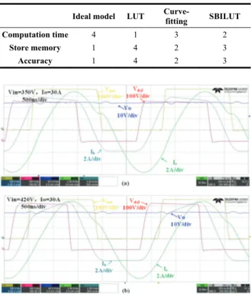
Fig. 10. Key waveforms under full load. (a) Vin=350V. (b) Vin=420V.
the efficiency of the SBILUT is slightly lower than the curve- fitting method, the SBILUT can reduce both the computation time and the memory consumption, which contributes to a low system cost. When compared with a LUT and curve-fitting, the performance of the SBILUT is balanced, which represents a tradeoff between the resources of the MCU and the calculation of the optimal phase. Thus, when comprehensively compared, the SBILUT is more adaptable and practical for BBLLC converters with an MCU.
V. E
XPERIMENTALR
ESULTSBased on the above analysis, a prototype is built to verify the proposed method presented in this paper. The specifications of the prototype are as follows. Input voltage Vin=350~420V, output voltage Vo=24V, output current
Io=15A~30A, and switching frequency fs=1MHz. The scales
for storing the optimal phase, kxij and kyij are the three 8*4
arrays used for the LUT and the SBILUT, considering tradeoffs between the memory size and the precision. In addition, these arrays only occupy 384 bytes in the MCU without affecting normal control.
Fig. 10(a) and Fig. 10(b) present operation waveforms of the BBLLC converter under a full load when Vin=350V and
Vin=420V. The amplitude of Vds2 varies with input change,
while Vds4 stays the same by regulating D. The phase between
ij xij ( i) yij ( j) f P f Q k x x k y y ( ) ( ) ij ij ij x in y o f P f Q k V k IFig. 11. Computation times of three methods.
S4 and S1 is regulated to provide enough energy for ZVS.
Here, it demonstrates that ZVS for the switches in a BBLLC converter can be achieved over a wide input range.
Fig. 11 shows waveforms of the sign voltage Vsign for
calculating the phase. When the MCU begins to calculate the optimal phase, the sign voltage Vsign is set to zero. In addition,
Vsign is set to a high level at the end of the calculation.
Therefore, the low state time can represent the calculation time of the optimal phase. The high state is the operating time for the sampling, state transition etc.
In consideration of the time for the MCU to pull up and pull down Vsign, the time is measured to be 0.255us. Then, the
computation time with the SBILUT, curve-fitting and LUT are measured. From the waveforms in Fig. 11, the average calculation times are 1.881us, 2.134us and 1.542us, respectively. In order to accurately obtain the computation times, the times to calculate the optimal phase need to be cut down by 0.255us, which are 1.626us, 1.879us and 1.287us, respectively. Therefore, this demonstrates that a shorter calculation time is achieved for the BBLLC converter with the SBILUT method, which can result in a 13.5% decrease in the computation time when compared with the curve-fitting method. For the high- frequency BBLLC converter, a shorter computation time can reduce the period of regulation for the phase, leading to a lower system cost. Since the period of this converter is 1us, the optimal phase is regulated at the end of the period. Taking the time for the MCU to update the optimal phase into consideration, the period of regulation for the phase with the SBILUT or LUT is 2us, while it changes to 3us with the curve-fitting method.
Experiment results for the dynamic responses of different methods are shown in the Fig. 12. When the load changes from 30A to 16A, the times to stabilize the output voltage are 1.65ms, 1.71ms and 1.81ms with different methods. Although the time with LUT is the shortest, the overshoot value of Vo is
the largest due to the low resolution of the phase. Since the time to calculate the optimal phase with the SBILUT is less than the curve-fitting method, the dynamic response time is less. As can be observed, the dynamic response performance of the SBILUT is superior to the other methods.
When it comes to the power loss of the converter, it mainly consists of conduction loss and hard-switching loss. If a smaller phase is adopted, the amplitude and the DC offset of
Fig. 12. Dynamic waveforms through three methods when Io
changes from 30A to 16A, Vin=385V.
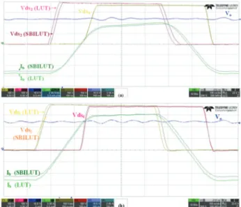
Fig. 13. Key waveforms of the conduction loss between different methods. (a) Input voltage 385V, output 24V,15A. (b) Input voltage 385V, output 24V 30A.
Ib increase, leading to conduction loss. Otherwise, Ib cannot
provide enough energy to realize ZVS of the switches. Since the optimal phases calculated with curve-fitting method and the SBILUT are close, the work efficiency and waveforms with these two methods are almost the same. Thus, key waveforms of the converter using the SBILUT and the LUT method are shown here to compare their merits and demerits.
Fig. 13 illustrates waveforms of Ib, the switch S2 drain-
source voltage Vds2, the switch S4 drain-source voltage Vds4
and the output voltage Vo. The green lines in Fig. 13(a) and
Fig. 13(b) represent the LUT method, while the dark green lines represent the SBILUT method. When compared with the optimal phase calculated through the SBILUT, the phase through the LUT method is smaller. As mentioned in Section II, if a smaller phase is adopted, the amplitude and the DC offset of Ib increase. Since the on-resistance of all the
switches is constant, a smaller phase through the LUT means that the RMS value of Ib is larger, which increases the
conduction loss by 4~5W.
Fig. 14 shows whether the ZVS of S1 or S2 is realized
under different working conditions. Similarly, Fig. 14(a) Fig. 14(c) use represent the SBILUT method, while Fig. 14(b) Fig.
Fig. 14. Key waveforms showing whether ZVS is realized in different methods. (a) and (b) input voltage 350V, output 24V 22.5A. (c) and (d) input voltage 420V, output 24V 22.5A. 14(d) represent the LUT method. Since the phase calculated through the LUT is larger than the optimal phase, the amplitude and the DC offset of Ib are not enough. As can be
seen, this cannot provide enough energy to fully charge Coss1
and Coss2 to realize ZVS of S1 and S2, which verifies the
former theoretical analysis. Thus, through the SBILUT method, the optimal phase can be obtained to increase the working efficiency.
Fig. 15 depicts converter efficiency curves under different working conditions. It demonstrates that the BBLLC converter operates with a high efficiency through the SBILUT method, which is close to that of the curve-fitting method. In addition, the efficiency with the SBILUT can be improved by about 1% when compared with the LUT. If the converter improves efficiency with the LUT, more data needs to be recorded, which consumes more memory of the MCU. Hence, the SBILUT can reduce memory consumption.
Fig. 15. Efficiency curve of a converter with different methods.
Fig. 16. Loss analysis with different methods.
Fig. 17. Utilization of MCU resources.
Fig. 16 shows a loss analysis under the full-load condition. Other losses take up about half of the total, which consists of the losses of the transformer, heat, driving and so on. Due to the accuracy of the optimal phase according to the SBILUT, the efficiency is slightly higher than the LUT. When compared with the LUT, the improvement of the SBILUT is analyzed as follow: the loss of the buck-boost inductor, the conduction loss of all the switches in the converter and the switching loss through always realizing ZVS. Meanwhile, in order to ensure the high-speed control of this converter, the curve-fitting method with its longer operation time is not appropriate.
Fig. 17 shows the utilization of the MCU resources. The gray part is for the case without the SBILUT, and the red part
350 400 450 500 550 600 650 700 750 0.92 0.93 0.94 0.95 0.96 0.97 0.98 Effi cie n cy
output power Po/W LUT SBILUT Curve-fitting
conduction loss turn-off Buck-Boost Inductor others
0% 1% 2% 3% Lo ss p erc en tage Curve-fitting SBILUT LUT B U S SRAM 12KB ADC1 ADC2 APB2 APB1 HRPWM Cortex M4 32-bit CPU 72MHz Flash 64KB
is the increased memory space for storing the data of the SBILUT. The other conventional control functions consist of self-check, soft startup, circuit protection and output voltage regulations. The code of these control functions takes around 16KB of flash space. The Read/Write variables take around 3.9KB of SRAM space, where the data for the SBILUT only consume 0.37KB of SRAM space. The CPU utilization is over 90%, demonstrating the full use of the MCU during the control process.
VI. C
ONCLUSIONSSince it is difficult for an MCU to obtain an ideal model of the most suitable phase due to the use of complex equations, other methods need to be chosen to calculate the optimal phase under different working conditions. The conventional curve-fitting method makes the MCU take a lot of time to operate, which increases the period of regulation for the phase. Additionally, although the LUT method is a simple way to reduce computation time, the accuracy of the phase and the memory space of the MCU need to be considered. Thus, an improved SBILUT method for calculating the phase is presented in this paper. This method is suitable for helping MCUs calculate the optimal phase quickly and accurately. The SBILUT combines a 2-D LUT with simplified bilinear interpolation, which results in a tradeoff between the accuracy of the optimal phase and the computation time. The proposed method also reduces memory consumption. Experimental results obtained with a 720W prototype are shown to verify the theoretical analysis. It can be seen that the proposed method is more applicable to BBLLC converters for the calculation of the optimal phase.
A
CKNOWLEDGMENTThiswork is supported by the Natural Science Foundation of Jiangsu Province (BK20171155).
R
EFERENCES[1] M. M. Jovanović and B. T. Irving, “On-the-fly topology- morphing control – Efficiency optimization method for LLC resonant converters operating in wide input- and/or output-voltage range,” IEEE Trans. Power Electron., Vol. 31, No. 3, pp. 2596-2608, Mar. 2016.
[2] S. M. S. I. Shakib and S. Mekhilef, “A frequency adaptive phase shift modulation control based LLC series resonant converter for wide input voltage applications,” IEEE Trans. Power Electron., Vol. 32, No. 11, pp. 8360-8370, Nov. 2017. [3] X. Sun, X. Li, Y. Shen, B. Wang, and X. Guo, “Dual-bridge LLC resonant converter with fixed-frequency PWM control for wide input applications,” IEEE Trans. Power Electron., Vol. 32, No. 1, pp. 69-80, Jan. 2017.
[4] H. Hu, X. Fang, F. Chen, Z. J. Shen, and I. Batarseh, “A
modified high-efficiency LLC converter with two transformers for wide input-voltage range applications,” IEEE Trans. Power Electron., Vol. 28, No. 4, pp. 1946-1960, Apr. 2013. [5] S. Lim, J. Ranson, D. M. Otten, and D. J. Perreault, “Two- stage power conversion architecture suitable for wide range input voltage,” IEEE Trans. Power Electron., Vol. 30, No. 2, pp. 805-816, Feb. 2015.
[6] C. Fei, Q. Li, and F. C. Lee, “Digital implementation of adaptive synchronous rectifier (SR) driving scheme for high-frequency LLC converters with microcontroller,” IEEE Trans. Power Electron., Vol. 33, No. 6, pp. 5351-5361, Jun. 2018.
[7] C. Fei, Q. Li, and F. C. Lee, “Digital implementation of light-load efficiency improvement for high-frequency LLC converters with simplified optimal trajectory control,” IEEE J. Emerg. Sel. Topics Power Electron., Vol. 6, No. 4, pp. 1850-1859, Dec. 2018.
[8] X. Sun, J. Qiu, X. Li, B. Wang, L. Wang, and X. Li, “An improved wide input voltage buck-boost + LLC cascaded converter,” in Energy Conversion Congress and Exposition, pp. 1473-1478, 2015.
[9] X. Sun, J. Qiu, X. Li, and Z. Luo, “An integrated buck- boost LLC cascaded converter with wide input voltage range Source” Proceedings of the Chinese Society of Electrical Engineering, Vol. 36, No. 6, pp. 1667-1673, Mar. 2016. (in Chinese)
[10] T. Pavlovic, T. Bjazic, and Z. Ban, “Simplified averaged models of DC–DC power converters suitable for controller design and microgrid simulation,” IEEE Trans. Power Electron., Vol. 28, No. 7, pp. 3266-3275, Jul. 2013. [11] H. Shi, X. Xiao, H. Wu, and K. Sun, “Modeling and
decoupled control of a buck–boost and stacked dual half-bridge integrated bidirectional DC–DC converter,” IEEE Trans. Power Electron., Vol. 33, No. 4, pp. 3534- 3551, Apr. 2018.
[12] X. Ren, Z. Guo, Y. Wu, Z. Zhang, and Q. Chen, “Adaptive LUT-based variable on-time control for CRM boost PFC converters,” IEEE Trans. Power Electron., Vol. 33, No. 9, pp. 8123-8136, Sep. 2018.
[13] D. R. Kincaid and E. W. Cheney, Numerical Analysis: Mathematics of Scientific Computing, 2002.
[14] B. Sahu and G. A. Rincon-Mora, “A low voltage, dynamic, noninverting, synchronous buck-boost converter for portable applications,” IEEE Trans. Power Electronics, Vol. 19, No. 2, pp. 443-452, Mar. 2004.
[15] X. Y. Ren, R. Xin-Bo, L. I. Ming-Qiu, H. Qian, and Q. H. Chen, “Dual edge modulated four-switch buck-boost converter,” in Proceedings of the Csee, Vol. 29, pp. 3635- 3641, 2009.
[16] A. Molina, K. Rajamani, and K. Azadet, “Concurrent dual-band digital predistortion using 2-D lookup tables with bilinear interpolation and extrapolation: Direct least squares coefficient adaptation,” IEEE Trans. Microw. Theory & Techniques, Vol. 65, No. 4, pp. 1381-1393, pp. 1-13, Apr. 2017.
[17] C. Vancea and S. Nedevschi, “LUT-based Image Rectification Module Implemented in FPGA,” in IEEE International Conference on Intelligent Computer Communication and Processing, pp. 147-154, 2007.
Qinsong Qian received his Ph.D. degree in the Electronics Engineering from Southeast University (SEU), Nanjing, China, in 2012. He joined the School of Electronic Science and Engineering, SEU, in 2012, where he is presently working as an Associate Professor. His current research interests include power converter topologies, simulations and digital control strategies.
Bowen Ren was born in Heilongjiang Province, China, in 1994. He received his B.S. degree in Electronics Engineering from Southeast University (SEU), Nanjing, China, in 2017, where he is presently working towards his M.S. degree in Electronics Engineering. His current research interests include DC-DC converters, simulations and digital control strategies.
Qi Liu received his B.S. degree in Electronics Engineering from Yangzhou University, Yangzhou, China, in 2015. He is presently working towards his Ph.D. degree in Electronics Engineering from Southeast University (SEU), Nanjing, China. His current research interests include digital control strategies for high-frequency and high-efficiency power conversions.
Chengwang Zhan was born in Anhui Province, China, in 1993. He received his M.S. degree in Electronics Engineering from Southeast University (SEU), Nanjing, China, in 2019. His current research interests include DC-DC converter digital control strategies.
Weifeng Sun received his B.S., M.S. and Ph.D. degrees in Electronics Engineering from Southeast University (SEU), Nanjing, China, in 2000, 2003 and 2007, respectively. Since 2006, he has been with the School of Electronic Science and Engineering, SEU, where he is presently working as a Professor. His current research interests include new power device designs, power ICs, power device modeling and power systems.