P1-112 /M. -Y. Lee
IMID 2009 DIGEST •
Abstract
We have developed a practical printing technology for the gate electrode of organic thin film transistors(OTFTs) by combining screen-printing with wet-etching process using nano-silver ink as a conducting material. The screen-printed and wet-etched Ag electrode exhibited a minimum line width of ~5 um, the thickness of ~65 nm, and a resistivity of ~10-6 Ω·cm, producing good geometrical and
electrical characteristics for gate electrode. The OTFTs with the screen-printed and wet-etched Ag electrode produced the saturation mobility of 0.13 cm2/Vs and current
on/off ratio of 1.79×10⁶, being comparable to those of
OTFT with the thermally evaporated Al gate electrode.
1. Introduction
The heavily doped Si wafer, the sputtered ITO and the thermally evaporated metal have been used for gate electrode of OTFT. However the conventional vacuum processes are not expected to satisfy the large-area deposition with the low-cost and at the low temperature and with the roll-to-roll process. Therefore, recently the additive solution processes such as ink-jet printing [1], roll-printing(gravure and flexography printing) [2] and transfer printing [3] with a metallic ink or a conducting polymer have been applied. But, these technologies could not meet the requirements of gate electrode due to the low conductivity and the poor geometrical characteristics and the process instability. On the other hand, the subtractive solution processes such as etching or lift-off for the solution processed metallic film such as spray coating, electroplating and spin coating [4,5] could fabricate the electrodes with the fine resolution, thin thickness, smooth surface and good uniformity. However the process complexity and the inefficiency usage of materials restricted their applications to gate electrodes. Especially, the spray coating,
electroplating and spin coating wasted the expensive conductive material and cause the environmental pollution.
In this paper, we have developed a practical printing process for the gate electrode of OTFT by combining a screen-printing with a wet-etching process where the nano-silver(Ag) ink was used for the conducting material. We could take the advantages of simplicity, environment-friendliness, and high material-efficiency by adopting the screen-printing process as a coating method of the uniform Ag film on the plastic substrate instead of the expensive vacuum evaporation.
2. Experimental
The nano-Ag ink was purchased from ANP Co.. The Ag content was 20wt% and the average diameter of Ag particles was about 30 nm. The Ag particles were mixed with the base solvent of terpineol(boiling point 214~220 ) achieving the viscosity of ~120 cps.
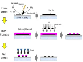
Fig. 1 shows the fabrication process of nano-Ag gate electrode by using the screen-printing and the wet-etching process. First, the PC(polycarbonate) plastic substrate was pre-annealed at 200 for 2 h in order to suppress thermal shrinkage during the subsequent processes, and then cleaned by the cleaning solution and the distilled water for 10 min, respectively. In order to enhance the adhesion between Ag film and PC substrate, the PVP(polyvinylphenol) solution [6] was spin-coated on the substrate after filtering through 0.2 um and then heated at 110 for 10 min and at 200 for 20 min. The thickness was about 350 nm. The Ag film was deposited onto the PVP-coated PC substrate by screen-printing process with the nano-Ag ink. Subsequently, it was cured at 200 for 60 min to eliminate the organic components
Fabrication of gate electrode for OTFT using
screen-printing and wet-etching with nano-silver ink
Mi-Young Lee
1and Chung-Kun Song
1,21Media device lab, Dong-A University,
2Dept. of Electronics Engineering, Dong-A University 840, Hadan-dong, Saha-gu, Busan 604-714, Korea
TEL:82-51-200-7711, e-mail: [email protected]
P1-112 / M. -Y. Lee
• IMID 2009 DIGEST
such as solvent and surfactant. We used the screen mask made of a stainless steel fabric with 640 mesh count/inch including an emulsion thin layer with the thickness of 5 um to form a thin thickness layer [7]. A photolithography process was carried out on the Ag film followed by wet etching process to pattern the film. Finally, the residual photo-resist was stripped off in acetone to obtain the final gate electrodes.
Fig. 1. The fabrication process of the gate electrode by screen-printing and wet-etching.
Additionally, to compare the results of the fabricated nano-Ag electrodes with the conventional vacuum-evaporated metal electrodes, Al electrodes with a thickness of ~70 nm were also fabricated on the same PVP-coated PC substrate by thermal vacuum evaporation and then wet-etching process.
To fabricate OTFTs, PVP dielectric layer with a thickness of about 350 nm was deposited on the gate electrodes with the same process as the PVP adhesion layer on the substrate. Subsequently, Au layer with a thickness of 45 nm was deposited for the S/D electrodes by thermal evaporation, and then patterned by lift-off process. Finally, pentacene layer with thickness of 45 nm was deposited on the S/D electrodes with a deposition rate of 0.3 /s in the base pressure less than 2×10⁻⁸ Torr through an aligned shadow mask to make the bottom contact OTFT devices.
3. Results and discussion
Fig. 2 shows the width of the gate electrode lines
fabricated by the screen-printing as well as by the thermal evaporation as the width was varied from 4 um to 50 um. For the case of the screen-printed lines, the lines were transferred as exactly as the layout when larger than 50 um, and the thickness was about 65 nm. However, as the width decreased from 50 um, the widths were reduced by 5~30% smaller than the layout. The reduction became serious as the width decreased smaller than 30 um, and finally the pattern disappeared when smaller than 5 um. This pattern reduction is resulted from the voids between Ag particles which were still existed even after sintering process at 200 . The acid of etchant penetrated into the voids in etching process and completely lifted off the narrow Ag line less than 5 um. On the contrary in the thermal evaporated Al lines there were not voids in Al film, therefore, such pattern loss was not frequently happened in thermal evaporated Al lines.
Fig. 2. The patterned line width (Wp) normalized to the layout line width (Wl) vs. the layout line width.
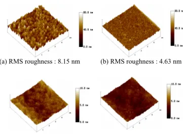
The surface roughness was measured by AFM and depicted in Fig. 3. The surface roughness of screen-printed Ag electrode was 8.15 nm, and 4.63 nm for the thermally evaporated Al electrode. The rough surface of gate electrode may degrade the electrical performance in OTFTs [5]. However, the rough surface was smoothed by coating PVP layer on the gate electrode as a gate dielectric. The surface roughness of PVP on Ag electrode was 0.7 nm which was comparable to 0.6 nm PVP on Al electrode as shown in Fig. 3c and d. This result was attributed to the thick and dilute PVP layer (~350 nm) which was five times thicker than the gate electrode (~65 nm).
P1-112 /M. -Y. Lee
IMID 2009 DIGEST •
(a) RMS roughness : 8.15 nm (b) RMS roughness : 4.63 nm
(c) RMS roughness : 0.7 nm (d) RMS roughness : 0.6 nm Fig. 3. AFM images of (a) the screen-printed Ag
electrode, (b) the thermally evaporated Al electrode, (c) the PVP dielectric layer on the Ag electrode, and (d) the PVP dielectric layer on the Al electrode.
The PVP layer provided a good step coverage to the gate electrode as shown in Fig. 4. The FE-SEM image of Fig. 4 shows the well covered PVP on the edge of Ag gate electrode. The good step coverage is very important to prevent the electrical shorts from occurring between gate and S/D electrodes.
Fig. 4. FE-SEM image of the cross-section of the screen-printed Ag electrode.
The resistivity of the nano-Ag electrode was about 7.7×10⁻⁶ Ω·cm meanwhile 1.5×10⁻⁵ Ω·cm for Al electrode. It was found that the screen-printed Ag electrodes with nano-Ag ink produced the better conductivity than the thermally evaporated Al electrodes if the organic components such as solvent
and surfactant are removed by curing.
The electrical performance parameters of OTFTs with channel width(W) of 400 um and channel length(L) of 20 um using the screen-printed Ag gate electrode and the thermally evaporated Al gate were summarized in Table 1, respectively. The mobility of 0.13 cm2/V·s of Ag gate is similar to 0.12 cm2/V·s of Al gate. This is resulted from the similar surface conditions of PVP gate dielectric of both OTFTs even though the gate electrodes are different. The similar surface conditions are attributed to the thin thickness (~65 nm) of Ag gate and also to the good step coverage of the thick PVP dielectric on the gate. TABLE 1. The electrical performance parameters
of OTFTs with the screen-printed Ag and the thermally evaporated Al gate electrodes Gate electrode Carrier mobility (cm2/V·s) Ion/off Vth (V) SS (V/dec) Ioff (pA/um) Screen-printed Ag 0.13 1.79×10⁶ 2.94 2.07 0.01 Evaporated Al 0.12 2.08×10⁶ -0.89 2.11 0.006
4. Summary
We developed a solution process for the gate electrodes of OTFTs, combining the screen printing with the wet etching process by using nano-Ag ink as the conducting material. The process is characterized by achieving the thin thickness of 65 nm and the high resolution of 5 um line width. The characteristics can be realized by selecting a suitable solvent such as terpineol with a high boil-point to prevent the solvent from being evaporated during printing process and by optimizing the mixing ratio of Ag contents to the solvent. The screen-printed Ag film had a high resistance to the acids of etchant, resulting in the high resolution. However, the pores of Ag film, which were originated from the voids between Ag nano-particles and were not disappeared even after curing at 200 oC, were the cause of patterns loss for the lines smaller than 5 um. The resistivity of the screen-printed Ag electrodes was ~10-6 Ω·cm better than that of the evaporated Al gate.
Although the process developed in this paper adopted the subtractive process such as lithography and etching beside the additive process of screen printing, it can replace the expensive evaporation process to implement the low cost and large area, the environmental friendliness, and the high material
P1-112 / M. -Y. Lee
• IMID 2009 DIGEST
efficiency, which are essential to the flexible applications.
5. Acknowledgements
This research was supported by a grant(F0004020) from the Information Display R&D Center, one of the 21st
Century Frontier R&D program funded by the Ministry of Knowledge Economy of Korean Government.
6. References
1. T. Kawase, T. Shimoda, C. Newsome, H. Sirringhaus, R. H. Friend, Thin Solid Films, 438-439, 279 (2003).
2. J-D. Jo, J-S. Yu, D-S Kim, K-Y Kim, and E-S Lee, IMID/IDMC/ASIA DISPLAY ’08 DIGEST, pp243-246 (2008).
3. B-D Chan, K-H Hsieh, S-Y Yang, Microelectron. Eng., 86, 586 (2009).
4. Y.G. Seol, J.G. Lee, N.-E. Lee, S-S Lee, J-H Ahn, Thin Solid Films, 515, 5065 (2007).
5. Y.G. Seol, J.G. Lee, N.-E. Lee, Org. Electron., 8, 513 (2007).
6. M.W. Lee, C. K. Song, J. Korean Phys. Soc., 47, 111 (2005).
7. J. Pan, G. L. Tonkay, A. Quintero, J. Electron. Manuf., 9, 203 (1999).